IC application · Voltage supervision without firmware
TPS3808: A Recovered Rail Must Stay Good Before RESET Releases
A voltage crossing a threshold is only the beginning of recovery. Build a small supervisor experiment, lower a divider-fed test voltage and watch how a new dip or manual reset starts the release interval again. Compare the open timing pin with a defined capacitor while keeping the chip's own supply valid.
1. What the supervisor adds to a comparator
An integrated circuit (IC) combines several circuit functions in one package. A voltage supervisor monitors a voltage and controls a reset signal with defined threshold and timing behavior. The exact part here is Texas Instruments (TI) TPS3808G01DBVR, the adjustable G01 variant in its DBV six-lead Small Outline Transistor (SOT-23) surface-mount package. Use a short, continuity-checked passive adapter; a similarly named fixed-threshold or automotive part is not an assumed replacement.
RESET is active-low: asserted means the IC pulls it LOW. Released means high impedance—the IC stops pulling, and an external resistor and load determine the voltage rise. It does not actively drive HIGH. MR means manual reset; pulling this input LOW requests reset independently of the sensed voltage. CT is the timing-capacitor pin. VDD is positive supply, SENSE is the monitored input and GND is their common ground reference.
The circuit needs no microcontroller or firmware. A host Python program below supplies nominal arithmetic and an ideal event model, not electrical simulation of the IC. No built prototype, measured threshold, delay qualification, target compilation or physical power-on behavior is claimed.
Units below are volts (V), milliamperes (mA), microamperes (µA), nanoamperes (nA), ohms (Ω), kilohms (kΩ), megaohms (MΩ), gigohms (GΩ), nanofarads (nF), picofarads (pF), seconds (s), milliseconds (ms) and microseconds (µs). A potentiometer is a resistor with a movable wiper. P1's clockwise (CW) and counterclockwise (CCW) ends and its wiper are numbered in the manufacturer's package drawing; J1 is a removable link, not a powered mode switch.
2. Derive every input from one valid supply
Logical terminals, not a footprint or breadboard placement. Every ground symbol denotes one common low-voltage net. The illustrated probe observes RESET; the manual-reset timing procedure specifies a second probe explicitly. Open full-size circuit · Download editable Scalable Vector Graphics (SVG).
Keep the supervisor powered in its specified operating range throughout the bench trial.
2 GND
Source return and all shown ground symbols
Common reference, including instruments.
5 SENSE
R1 64.9 kΩ ±1% from TP_VTEST; R2 10 kΩ ±1% and C1 1 nF ceramic to GND
Monitor a divided, filtered test voltage.
3 MR
Normally open momentary SW1 to GND
The IC's internal pull-up returns MR HIGH when released.
4 CT
J1 absent: open; J1 fitted: C2 100 nF ±5% to GND
Two separately powered-down assembly configurations.
1 RESET
R3 100 kΩ ±1% to the same VDD; high-impedance scope to GND
Open-drain output with an explicit pull-up and return.
P1 is a Bourns 3386P-1-103LF, 10 kΩ single-turn cermet part, with a ceramic-and-metal resistive element: terminal 3 to 3.30 V, terminal 1 to GND, terminal 2 as TP_VTEST. Check the exact P-style physical drawing before soldering. The wiper's actual loaded voltage is the test variable; its rotation fraction is not a calibrated voltage scale.
Use Vishay MRS25 metal-film examples MRS25000C6492FCT00 for R1, MRS25000C1002FCT00 for R2 and MRS25000C1003FCT00 for R3, all ±1%. C2 is the nonpolar WIMA MKS2C031001A00JSSD, 100 nF ±5%, 63 V. C1 and C3 are ordinary suitable low-voltage ceramic parts; their effective values, leakage and layout still matter. Keep CT particularly short and clean, without a scope probe attached during the comparison.
A current-limited bench source set to 3.30 V with a 10 mA limit is sufficient for this low-current resistor fixture; verify its actual output before connection. This limit is not a voltage regulator or an IC protection guarantee. VDD, P1 and the RESET pull-up all use that same source. There is no separately powered SENSE source or pull-up to back-power an unpowered chip. Remove all power before changing J1, then allow the nodes to discharge.
3. Calculate the falling threshold, not a magic knob position
The G01 nominal negative-going SENSE threshold, VIT, is 0.405 V. The divider maps that to a larger TP_VTEST voltage. Input current adds a small error. Define positive input current as current flowing into SENSE:
The resistance-capacitance (RC) estimate omits the potentiometer's source resistance, instrument load, adapter capacitance and component variation. The 1 nF filter reduces sensitivity to short disturbances but also changes their shape. This experiment uses slow voltage movement and manual reset; it does not qualify a minimum detectable supply glitch.
Do not apply the headline 0.5% accuracy to this adjustable G01. The current datasheet gives ±2% negative-going threshold accuracy over its specified conditions, with the typical G01 entry ±1%. The code evaluates all corners of G01 ±2%, each divider resistor ±1% and SENSE input current ±25 nA. It obtains a falling TP_VTEST interval of approximately 2.92017–3.14992 V. This includes the specified IC temperature contribution; additional resistor/source drift outside the entered tolerances and probe effects are not added.
Hysteresis is a separation between falling and rising thresholds that helps avoid repeated switching near a boundary. For G01, the datasheet lists 1.5% typical and 3% maximum of VIT, with no stated minimum. Thus a typical modeled rising point is about 3.07895 V using the nominal divider. It is an assumption, not a guaranteed minimum gap. At the upper falling corner, adding the stated 3% hysteresis scale reaches roughly 3.244 V before other errors. Verify that the loaded wiper can reach a sufficient measured recovery voltage without exceeding the common supply.
4. CT controls release after both causes clear
A low SENSE input or low MR asserts RESET. Recovery starts only when MR is HIGH and SENSE is above VIT plus its hysteresis voltage. The internal timer then holds RESET LOW. A renewed assertion discharges the timing capacitor and requires a new interval; a short earlier good period does not accumulate credit.
With CT open, the datasheet's switching table specifies 12 ms minimum, 20 ms typical and 28 ms maximum under its stated load, voltage and temperature conditions. Open does not mean a floating breadboard wire may be arbitrarily long. The pin and adapter have capacitance, and the manufacturer warns that stray capacitance changes timing.
For an external capacitor, the primary nominal equation is:
nominal delay_s = CT_nF / 175 + 0.0005
100 nF → about 0.571929 s
95..105 nF → about 0.543357..0.600500 s
These are equation results, not guaranteed delay limits.
The current Rev N table changed two older entries: the small-capacitor row is now 130 pF, and the 180 nF row is 0.62 / 1.03 / 1.44 s minimum / typical / maximum. There is no tabulated guaranteed 100 nF interval to invent by interpolating those rows. Capacitor tolerance alone cannot turn the nominal formula into a full timing guarantee. At least 100 pF nominal is required for capacitor recognition; that recognition boundary is different from the revised 130 pF test row.
TI describes a nominal 220 nA timing current charging toward about 1.23 V. Leakage is significant compared with such a small current. WIMA specifies at least 10 GΩ insulation resistance for this 63 V / 100 nF family at its +20 °C test conditions. Treating that resistance as a simple model gives about 0.123 nA at 1.23 V, but that calculation does not measure actual CT leakage, dielectric absorption, contamination or behavior at every temperature. A leaky adapter, capacitor or probe can change the delay substantially. The film part is selected as a documented low-leakage candidate; actual qualification remains necessary.
5. A released output still has a load
The recommended RESET pull-up range is 10 kΩ to 1 MΩ; this fixture uses 100 kΩ. At nominal 3.30 V it asks for about 33 µA when LOW, not a directly connected light-emitting diode load. The table's output LOW guarantee is conditional—for example, up to 0.4 V at a 1 mA sink with VDD at least 1.8 V. Do not replace that condition with a claim of an ideal zero-volt output.
The RESET leakage maximum of 300 nA corresponds to as much as 30 mV across 100 kΩ under that leakage specification. A 10 MΩ instrument also loads the pull-up: an ideal 100 kΩ / 10 MΩ divider would give roughly 3.267 V before other effects. Probe capacitance affects the released voltage rise, while the IC's release event is its transition to high impedance. Keep those times separate in a scope interpretation.
The internal MR pull-up is 70–90 kΩ in the stated table. A grounded contact requests reset without a second powered driver; the released contact lets that bias restore HIGH. Real contact bounce may produce several reset requests and lengthen the observed interval. That is an observation to record, not a reason to call the button a precise pulse generator.
Recommended VDD operation is 1.7–6.5 V. The datasheet separately describes lower-voltage power-on-reset behavior with specific output-current and supply-rise conditions; below the power-on-reset voltage it calls RESET undefined. This bench keeps VDD at 3.30 V. It does not sweep VDD or generalize a conditional low-voltage assertion to this pull-up/load. Absolute maximum ratings are stress limits, not an alternative operating region.
6. Read the constructed event trace carefully
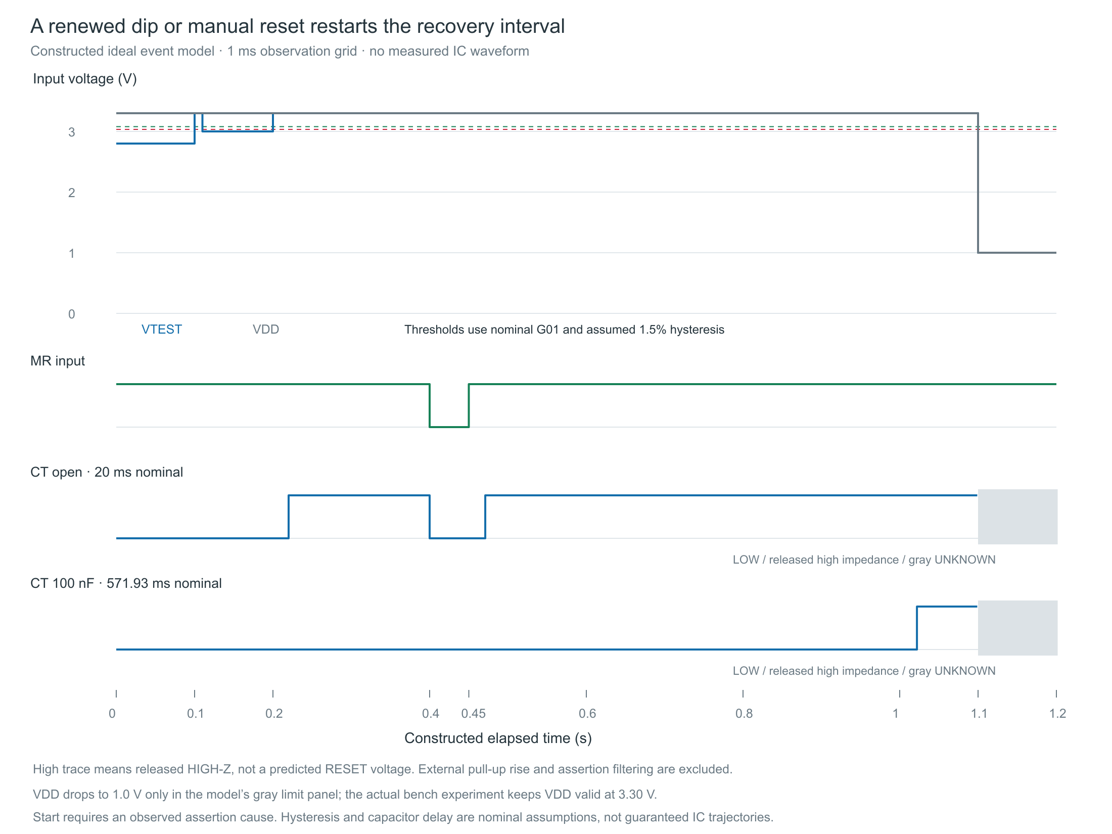
The host model uses an ideal hysteretic comparator and selectable delay. It omits analog filtering, propagation delay, capacitor leakage, output rise and physical power ramps. It requires an observed assertion cause before predicting a release; this deliberately avoids inventing a known startup state. Values in the hysteresis band preserve the prior ideal comparator state.
Constructed from the complete supplied event model on a 1 ms grid, not an IC measurement. Red dashed is the nominal falling threshold; green dashed is the assumed rising threshold. A high output trace means released high impedance, sometimes written HIGH-Z, not a predicted pin voltage. Gray is UNKNOWN. Open full-size timing diagram · Download editable SVG.
The 100 nF model's nominal deadline after the final MR release at 0.45 s is approximately 1.021929 s. The 1 ms grid first reports release at 1.022 s; that difference is observation-grid quantization. At 1.1 s the model deliberately moves VDD to 1.0 V and returns UNKNOWN. That gray illustration is outside the actual valid-VDD experiment and does not claim the physical IC necessarily drives LOW or releases there.
The model only accepts an increasing elapsed time between 0 and 60 s and a same-supply test voltage. Its time bound also prevents a huge floating-point timestamp from rounding a positive delay into the same number. It has no clock input or hardware control: do not interpret its event times as measurements, supply supervision or firmware protection.
7. Complete host calculator and finite model
Save this file as tps3808_release_model.py on a host computer and run python tps3808_release_model.py > model-report.json. It prints a finite report with two 1201-row traces, nominal calculations and explicit missing guarantees. It does not connect to any pins or program the IC.
"""Host-only TPS3808 lesson arithmetic and an explicitly ideal event model.
No GPIO, IC emulator, analog transient solver or firmware is provided.
"""
import itertools
import json
import math

TOP_OHM = 64900.0
BOTTOM_OHM = 10000.0
VIT_V = 0.405

def finite(x):
    if isinstance(x, bool) or not isinstance(x, (int, float)) or not math.isfinite(x):
        raise ValueError('FINITE_NUMBER_REQUIRED')
    return x

def falling_threshold(top=TOP_OHM, bottom=BOTTOM_OHM, vit=VIT_V, sense_A=0.0):
    """Current positive into SENSE; fixture-domain calculation, not arbitrary parts."""
    top,bottom,vit,sense_A=map(finite,(top,bottom,vit,sense_A))
    if not 60000 <= top <= 70000 or not 9000 <= bottom <= 11000:
        raise ValueError('FIXTURE_RESISTORS')
    if not .39 <= vit <= .42 or abs(sense_A)>25e-9:
        raise ValueError('FIXTURE_THRESHOLD_OR_CURRENT')
    return vit*(1+top/bottom)+sense_A*top

def threshold_corners():
    values=[falling_threshold(a,b,v,i) for a,b,v,i in itertools.product(
        [TOP_OHM*.99,TOP_OHM*1.01], [BOTTOM_OHM*.99,BOTTOM_OHM*1.01],
        [VIT_V*.98,VIT_V*1.02], [-25e-9,25e-9])]
    return {'falling_nominal_V':falling_threshold(),
            'falling_corner_interval_V':[min(values),max(values)],
            'includes':'G01 threshold ±2%, each resistor ±1%, input current ±25nA',
            'excludes':'resistor/source drift outside entered tolerances, measured values, probe effects and rising hysteresis'}

def nominal_delay(cap_nF):
    cap_nF=finite(cap_nF)
    if not 95 <= cap_nF <= 105:
        raise ValueError('100NF_FIXTURE_ONLY')
    return cap_nF/175+.0005

class ReleaseModel:
    """Slow-input ideal comparator/timer policy, NOT a physical IC simulation.
    Requires an observed assertion cause before making any release prediction.
    Hysteresis and delay are explicit illustrative assumptions; no glitch model.
    """
    def __init__(self,delay_s,hysteresis_fraction=.015):
        delay_s,hysteresis_fraction=map(finite,(delay_s,hysteresis_fraction))
        if not .001 <= delay_s <= 10 or not 0 <= hysteresis_fraction <= .03:
            raise ValueError('MODEL_PARAMETER')
        self.delay=delay_s
        self.fall=falling_threshold()
        self.rise=self.fall*(1+hysteresis_fraction)
        self.last=None
        self.good=None
        self.primed=False
        self.deadline=None
        self.bad=False
    def observe(self,t_s,vdd,vtest,mr_high=True):
        if self.bad:
            raise ValueError('MODEL_INVALID')
        try:
            t_s,vdd,vtest=map(finite,(t_s,vdd,vtest))
            if not 0 <= t_s <= 60 or (self.last is not None and t_s<=self.last):
                raise ValueError('TIME_WITHIN_60S_AND_INCREASING')
            if not 0 <= vdd <= 6.5 or not 0 <= vtest <= vdd or type(mr_high)is not bool:
                raise ValueError('COMMON_SUPPLY_INPUT')
        except BaseException:
            self.bad=True
            raise
        self.last=t_s
        if not 1.7 <= vdd <= 6.5:
            self.good,self.primed,self.deadline=None,False,None
            state='UNKNOWN'
        else:
            if vtest<self.fall:self.good=False
            elif vtest>self.rise:self.good=True
            # In the hysteresis band retain the previous ideal comparator state.
            if not mr_high or self.good is False:
                self.primed,self.deadline=True,None
                state='ASSERTED_LOW'
            elif self.good is None or not self.primed:
                state='UNKNOWN'
            else:
                if self.deadline is None:self.deadline=t_s+self.delay
                state='RELEASED_HIGH_Z' if t_s>=self.deadline else 'DELAYING_LOW'
        return {'t_s':t_s,'VDD_V':vdd,'VTEST_V':vtest,'MR_high':mr_high,
                'state':state,'deadline_s':self.deadline,
                'physical_RESET_voltage_V':None,'physical_prediction':False}

EVENTS=[(0.,2.8,True),(.10,3.3,True),(.11,3.0,True),(.20,3.3,True),
        (.40,3.3,False),(.45,3.3,True)]

def constructed_trace():
    """One-millisecond observation grid with ideal step input events."""
    output={}
    for name,delay in [('open_nominal',.020),('100nF_nominal',nominal_delay(100))]:
        m=ReleaseModel(delay);rows=[]
        for ms in range(1201):
            t=ms/1000
            vtest,mr=2.8,True
            for at,v,b in EVENTS:
                if at<=t:vtest,mr=v,b
            vdd=3.3
            if ms>=1100:vdd,vtest=1.0,1.0
            rows.append(m.observe(t,vdd,vtest,mr))
        output[name]=rows
    return {'scope':'Constructed ideal slow-input state trace, not sensor/IC measurements',
            'sample_grid_ms':1,'hysteresis_fraction_assumed':.015,
            'output_rise_and_assertion_propagation_modeled':False,'profiles':output}

def main():
    result={'threshold':threshold_corners(),
            'CT_open_datasheet_min_typ_max_ms':[12,20,28],
            '100nF_formula_nominal_s':nominal_delay(100),
            '95to105nF_formula_only_s':[nominal_delay(95),nominal_delay(105)],
            '100nF_guaranteed_min_max_s':None,
            'CT180nF_table_min_typ_max_s':[.62,1.03,1.44],
            'trace':constructed_trace(),'hardware_tested':False,'firmware_built':False}
    print(json.dumps(result))
    return result

if __name__=='__main__':main()
The single experiment and host-test archive includes the program, tests, original graphics, constructed data and blank log. Extract it and run python test_release_model.py. Checks execute the supplied calculator and event model, including threshold corners, delay restart, hysteresis-band history, unknown supply state, malformed input and the exact command-line invocation. They are not target firmware compilation or electrical validation.
8. Four observations with no filled-in results
With power removed, identify U1's pin 1 and the exact DBV top view. Check every adapter route and P1's P-style terminals. Assemble the divider, filter, bypass and pull-up; leave J1 absent. Verify all instrument returns connect only to this circuit's common GND.
Set the source to 3.30 V and a 10 mA current limit before connection. Measure loaded VDD at pins 6 and 2. Set the wiper low enough to assert reset; do not begin by assuming startup produced a particular state.
Measure TP_VTEST relative to GND while slowly increasing and decreasing it. Record the falling assertion and rising recovery readings separately, along with instrument loading. A threshold measurement is not the timing measurement; avoid interpreting the 1 nF filter as a guaranteed glitch catcher.
For the manual-reset timing observation, hold TP_VTEST at a verified good value. On a two-channel high-impedance scope, connect one tip to pin 3 MR and the other to pin 1 RESET, with both reference leads at GND. Trigger on MR release and compare it with RESET voltage rise. Record probe resistance/capacitance, trigger definition and any contact bounce. The functional drawing illustrates the RESET channel; the second tip is a measurement connection at the named MR terminal.
Remove all power, fit J1 to C2, and repeat after checking the circuit. Compare a roughly half-second nominal recovery with the open-pin case. Leave CT unprobed; if you probe it in a separate investigation, record that changed load instead of reusing the original result.
During a pending recovery, press MR again, or deliberately return TP_VTEST below its falling threshold. Confirm the complete later interval begins anew. Use a sufficiently slow, clearly observed change; neither hand movement nor a mechanical contact qualifies microsecond rejection behavior.
Disconnect power afterward. Keep actual observations in the blank worksheet, presently header only. Retain failed or ambiguous captures rather than replacing them with the nominal line.
Use an oscilloscope to distinguish the MR edge from the RESET rise. A slow voltmeter can show the static state but cannot establish a 12–28 ms release interval. No processor is connected in this experiment, and a well-behaved reset signal would not by itself repair an unstable power source.
9. Challenge: may two short good periods add up?
The nominal capacitor model needs 571.93 ms after recovery. SENSE becomes good for 400 ms, dips below its falling threshold, and then becomes good for another 200 ms. May RESET release because the total good time exceeds the nominal delay?
Show the answer
No. The new assertion discharges the timing capacitor and restarts qualification. The final good period must satisfy a complete new delay after both MR and SENSE clear. The numerical example uses a nominal model; actual capacitor, timing-current, threshold, leakage and output-load behavior still require the exact datasheet conditions and measurements.
10. Primary documents and downloads
TI exact TPS3808G01DBVR orderable and TPS3808 SBVS050N, August 2026, §§5–8 and revision history. Current Rev N changed the 130 pF and 180 nF timing entries; cached Rev M results were not substituted. No separate applicable errata file was found in this bounded product-document check, not ruled out universally.
WIMA MKS2, March 2026, 100 nF / 63 V row, ±5% ordering completion and insulation test conditions.
Bourns 3386, exact P-style pin geometry, 10 kΩ code and electrical limits; Vishay MRS16/MRS25, ±1% family and resistance ordering.