📌 What is EasyEDA?
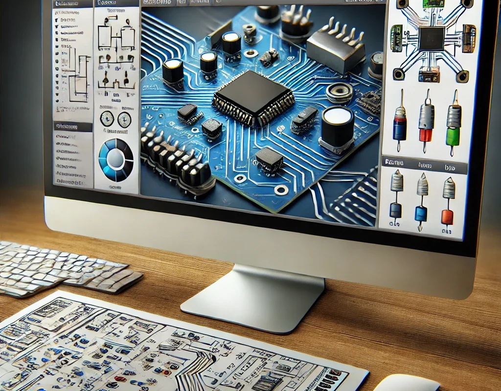
EasyEDA is a cloud-based electronic circuit and PCB design tool that makes creating schematics, designing PCBs, and even ordering manufactured boards super easy! 🏗️💡
It’s perfect for hobbyists, makers, and professionals, offering an AI-powered design assistant, real-time collaboration, and seamless integration with manufacturing services. No installation needed – just open a browser and start designing! 🌍💻
⚡ 1. Why Choose EasyEDA? (Key Features)
✅ Full cloud-based schematic & PCB editor – No downloads required!
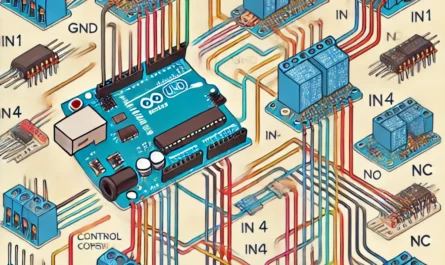
✅ Massive library of components – Resistors, ICs, connectors, sensors, and more! 🛠️
✅ Real-time collaboration – Work with a team on the same PCB from anywhere!
✅ AI-assisted circuit design – Auto-routing & component placement optimization! 🤖
✅ Seamless integration with JLCPCB – Order your board with one click! 🏭
✅ SPICE circuit simulation – Test circuits before building them! 🔄
🎨 2. How to Use EasyEDA (Step-by-Step)
🔹 Step 1: Open EasyEDA & Create a New Project
1️⃣ Go to EasyEDA Website 🌍
2️⃣ Sign up/log in to save your projects.
3️⃣ Click “New Project” and choose Schematic Capture or PCB Layout.
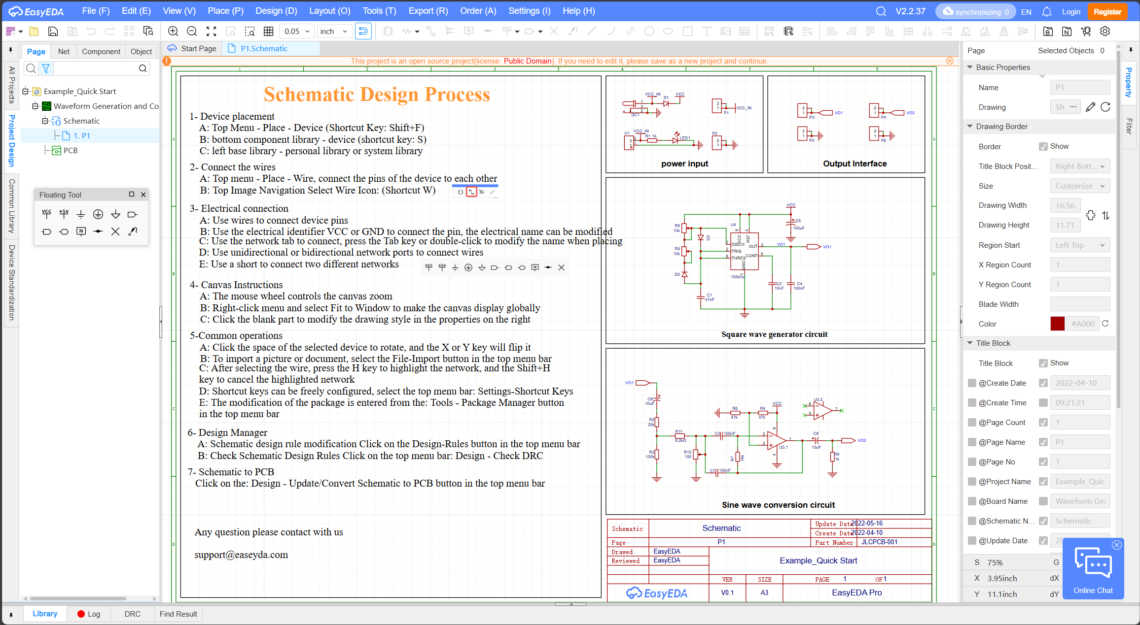
🔹 Step 2: Create a Schematic
1️⃣ Drag & drop components from the massive parts library.
2️⃣ Use wire connections to link components.
3️⃣ Add labels & values to define component ratings.
4️⃣ Simulate the circuit to ensure it works before making the PCB.
💡 Pro Tip: EasyEDA supports SPICE simulation, so you can test voltage, current, and circuit behavior before printing a PCB! 🔥
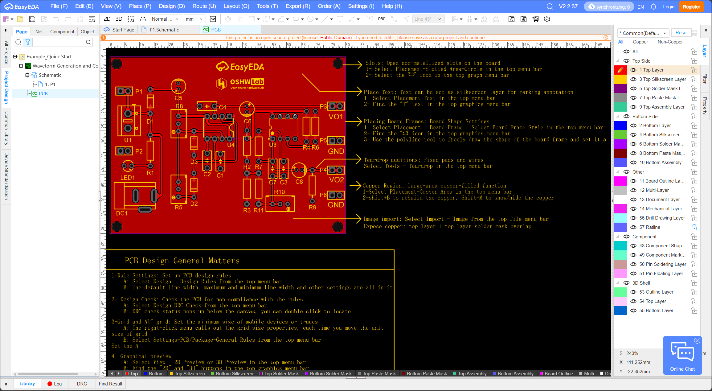
🔹 Step 3: Convert to PCB Layout
1️⃣ Click “Convert to PCB” to switch from schematic to board design.
2️⃣ Arrange components on the PCB layout manually or let AI auto-place them! 🤖
3️⃣ Route traces manually or use the AI auto-router.
4️⃣ Define PCB size, shape, and layer count.
💡 AI auto-routing can optimize signal paths and reduce interference for high-speed circuits! 🚀
🔹 Step 4: Generate Gerber Files & Order Your PCB
1️⃣ Click “Generate Gerber Files” – these files are needed for PCB manufacturing.
2️⃣ Directly order from JLCPCB (EasyEDA’s official partner) or export for other manufacturers.
3️⃣ Choose material, layer count, and solder mask color.
4️⃣ Submit your order and get your custom PCB shipped! 📦
✅ Super fast & cheap! JLCPCB offers 5 PCBs for just $2 – insane pricing for makers! 💰
🔧 3. AI-Powered Features in EasyEDA
EasyEDA is not just another PCB tool – it integrates AI to simplify the design process! 🤖
🔹 AI Auto-Routing
✅ Automatically connects traces based on signal integrity and power needs!
✅ Reduces noise & improves PCB efficiency.
✅ Saves hours of manual routing time!
🔹 AI-Based Component Placement
✅ Optimizes component layout for heat dissipation and signal clarity!
✅ AI arranges resistors, capacitors, ICs for minimal interference.
🔹 AI-Powered Component Sourcing
✅ Suggests alternative components if a part is out of stock.
✅ AI checks JLCPCB’s inventory to prevent ordering issues.
💡 This makes EasyEDA one of the smartest PCB design tools for fast prototyping! 🚀
📌 4. Why Choose EasyEDA Over Other PCB Tools?
🔹 EasyEDA vs. KiCad
| Feature | EasyEDA | KiCad |
|---|---|---|
| Cloud-Based? | ✅ Yes, works in browser! | ❌ No, requires install |
| AI Auto-Routing? | ✅ Yes | ❌ No |
| Simulation? | ✅ Yes, built-in SPICE | ✅ Yes, but harder to use |
| Component Sourcing? | ✅ Auto-suggests parts via JLCPCB | ❌ Manual sourcing |
| Best For? | Hobbyists & rapid PCB prototyping | Professional, open-source projects |
🔹 EasyEDA vs. Altium Designer
| Feature | EasyEDA | Altium Designer |
|---|---|---|
| Pricing | ✅ Free (with premium options) | ❌ Very expensive! 💰 |
| Cloud-Based? | ✅ Yes! | ❌ No, requires install |
| AI Features? | ✅ Yes (auto-routing, placement, sourcing) | ✅ Advanced AI tools but complex |
| Manufacturing Integration? | ✅ JLCPCB one-click ordering | ✅ Requires manual setup |
| Best For? | Hobbyists, startups, & rapid prototyping | Large-scale professional projects |
💡 EasyEDA is the BEST choice if you want a free, AI-enhanced, and cloud-based PCB tool! 🌍🔥
🚀 5. Who Should Use EasyEDA?
✅ Makers & Hobbyists – No expensive software needed!
✅ Students & Beginners – Easy learning curve with AI guidance!
✅ Startups & Small Businesses – Fast PCB design & manufacturing!
✅ Anyone Who Wants Cloud-Based PCB Design – No installation, no compatibility issues!
🔥 6. Final Verdict: Why EasyEDA is the Future of PCB Design
✔ Cloud-based & AI-enhanced – No software installs, works anywhere! ☁️
✔ Massive component library – Over 1 million+ parts! 🔧
✔ SPICE simulation – Test circuits before manufacturing! 📊
✔ AI-powered auto-routing & component placement – Saves hours of work! 🤖
✔ One-click manufacturing with JLCPCB – No need to search for factories! 🏭
💡 Final Thought:
🔥 If you want a free, fast, and modern PCB tool that’s integrated with AI and manufacturing, EasyEDA is the ultimate choice in 2025! 🚀