A pushbutton is a mechanical contact, not a perfect source of one electrical edge. On a close-up recording, a single press can contain several brief closures and openings. A digital counter may interpret them as several events. This experiment builds a contact conditioner from one logic chip, two timing resistors and a capacitor. The resistor–capacitor (RC) network smooths brief contact changes before the gate decides. It also gives you a second, slower experiment: measure the two input voltages at which the same gate changes its mind.
Verification: this is a locally reviewed circuit with calculated results and a host-side mathematical model. It has not been physically assembled or measured for this article. There is no microcontroller firmware. The LED shows the stable state; an oscilloscope is needed to demonstrate the number and timing of edges.
Choose the exact chip and supply
Use Texas Instruments SN74HC14N, the 14-pin plastic dual-inline package (PDIP). An integrated circuit, or IC, contains multiple electronic functions inside one package. This one contains six independent inverting Schmitt-trigger gates. We use two gates and deliberately connect the four unused inputs to ground. The N suffix here identifies TI’s through-hole package; it does not mean a narrow surface-mount package.
For the numerical experiment, set a regulated, current-limited bench supply to 4.50 V before connecting the board. Start with a 20 mA limit. Ground, marked GND, is the common return and voltage reference. Use only this small standalone circuit at first. Its output is a roughly 4.5 V logic signal, so it must not be connected directly to a 3.3 V-only Pico or ESP32 general-purpose input/output (GPIO) pin.
| Reference | Part | Job |
|---|---|---|
| U1 | TI SN74HC14N, PDIP-14 | Turn a slowly changing input into a distinct logic state. |
| R1 / R2 | 100 kΩ / 10 kΩ, each 1%, 0.25 W | Charge the timing capacitor; limit its discharge through the button. |
| C1 | 1 µF film, ±10%, rated at least 16 V | Average short contact interruptions. Film avoids the large leakage and voltage-dependent capacitance of some alternatives. |
| R3 / D1 | 2.2 kΩ, 1%; ordinary low-current red LED | Limit the light-emitting diode’s current and display a press. |
| C2 / C3 | 100 nF ceramic / 10 µF electrolytic, at least 10 V | Local supply bypass and bulk supply support. C3 has polarity. |
| S1 | Normally open pushbutton | Connect the bottom of R2 to GND when pressed. |
| P1 / R4 | 10 kΩ linear potentiometer / 1 kΩ | Only for the later threshold experiment. |
A breadboard, short wires and a voltmeter are enough for the steady-state and threshold experiments. To inspect bounce, add a two-channel oscilloscope with ×10 probes. A logic analyser can count clean output edges, but cannot show the slowly changing capacitor voltage. Check its allowed input voltage before connecting it.
Wire the conditioner
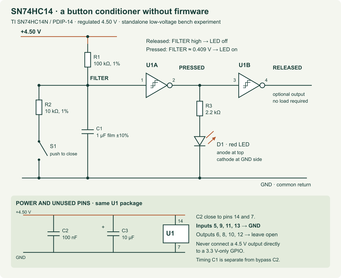
- With power disconnected, put U1 across the breadboard’s centre gap. Viewed from above with the notch at the top, pin 1 is top-left. Count down to pin 7, then up the right side from pin 8 to pin 14. Check the moulded notch or pin-one mark, not the printed lettering direction alone.
- Connect U1 pin 14 to +4.50 V and pin 7 to GND. Place C2 directly between these two supply nets near the chip. Connect C3 across the rails, positive to +4.50 V and negative to GND. Bridge split breadboard power rails where necessary.
- Create the FILTER node at U1 pin 1. Connect R1 from +4.50 V to FILTER and C1 from FILTER to GND. Connect R2 from FILTER to S1, with S1’s other contact at GND. R2 is in series with the switch, not across C1.
- U1 pin 2 is PRESSED. Connect it through R3 to the LED anode; connect the cathode to GND. The cathode normally has the shorter lead and a flat on the case, but check the actual LED.
- Connect pin 2 to pin 3. Pin 4 becomes RELEASED, an optional inverted copy for a high-impedance measuring input. Leave it unconnected if unused.
- Tie unused input pins 5, 9, 11 and 13 directly to GND. Leave unused output pins 6, 8, 10 and 12 open. Never join two outputs together or tie an output directly to a supply rail.
Many four-legged tactile buttons permanently join the two legs on each side. A continuity check with the button unpowered identifies the two separate contact groups. Using two legs from the same permanently joined group makes this circuit look permanently pressed. The diagram represents the actual contact, not the physical leg layout of every button.
Why two thresholds help
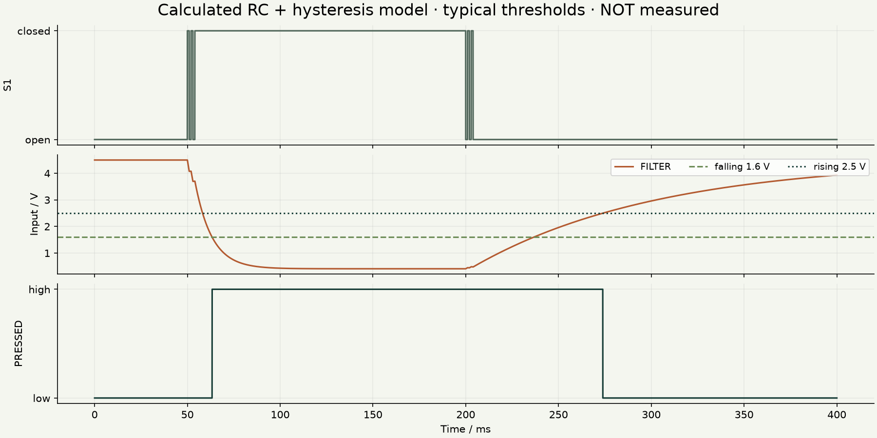
An inverter produces a high output for a low input and a low output for a high input. A Schmitt input adds hysteresis: its decision depends on which direction the input is moving and the previous state. Rising FILTER voltage must cross the upper threshold to turn PRESSED low. Falling FILTER voltage must cross the lower threshold to turn it high again. A small wobble between those thresholds keeps the previous output.
At 4.5 V, the TI specification gives an upper threshold of 1.55–3.13 V (2.5 V typical) and a lower threshold of 0.9–2.45 V (1.6 V typical). Hysteresis is at least 0.4 V. These are population limits, not adjustable setpoints. Do not combine overlapping independent extrema into a fictional chip with its lower threshold above its upper threshold. Use the two measured thresholds from your particular gate when predicting its timing. See TI SCLS085L, sections 4–5 and 7–8.
The supported supply range is 2–6 V, with inputs operated between GND and the supply. The 7 V supply and ±25 mA output figures in the absolute-maximum table are stress limits, not design targets. At 4.5 V the output levels are specified at a 4 mA load; our LED circuit draws much less. Slow Schmitt-input transitions are supported, but may increase supply current. The quoted threshold limits belong to 4.5 V; changing the rail requires revisiting the prediction.
Calculate both directions, not just R × C
With S1 released, C1 charges through R1. Its time constant is 100 kΩ × 1 µF = 100 ms. A time constant describes the shape of an exponential; it is not automatically the switch delay. When S1 closes, R1 remains connected to the supply while R2 connects to ground. The capacitor now sees a divider and a different resistance.
Held-press voltage:
Vclosed = 4.5 × 10k / (100k + 10k) = 0.409 V

Resistance seen by C1 while pressed:
Rparallel = 100k × 10k / (100k + 10k) = 9.091 kΩ
Press time constant = Rparallel × C1 = 9.091 ms

For either fixed contact state:
V(t) = Vfinal + (Vstart − Vfinal) × exp(−t / time_constant)

From fully released, using the typical lower threshold:
tpress = 9.091 ms × ln[(4.5 − 0.409) / (1.6 − 0.409)]
       = 11.22 ms

From fully held, using the typical upper threshold:
trelease = 100 ms × ln[(4.5 − 0.409) / (4.5 − 2.5)]
         = 71.56 ms
The nominal held voltage is below the lowest specified lower threshold, so a sustained press has room to reach the required state. The release rises toward 4.5 V, above the highest upper threshold. Our component-corner calculation, with 1% resistors and 10% capacitance, predicts roughly 5.63–21.51 ms for a settled press and 28.97–121.74 ms for a settled release at exactly 4.5 V, ignoring leakage and probe loading. These are calculated endpoint envelopes, not a measured timing guarantee.
Initially, a press can discharge C1 through 10 kΩ at at most about 4.5 / 10,000 = 0.45 mA nominal. Removing R2 creates a brief large capacitor-discharge current limited mainly by the switch and wiring. Holding the switch consumes about 4.5 / 110,000 = 40.9 µA in the divider. With an assumed 2 V LED drop, LED current is approximately (4.5 − 2) / 2,200 = 1.14 mA; actual output voltage and LED drop reduce or change that figure.
A meter also becomes part of the circuit. A 10 MΩ input across FILTER pulls its released level to about 4.455 V and changes the charging resistance to about 99.0 kΩ. A 1 MΩ probe loads it more. Use a ×10 scope probe, keep its ground lead short, and record your probe or meter input resistance. Excess capacitor leakage can keep the released voltage too low. Treat a badly leaking or unknown electrolytic as a different design, not a like-for-like C1 replacement.
Three bench experiments
1. Establish the steady states
Power up with S1 released and wait one second. Measure the supply first, then FILTER, PRESSED and RELEASED. FILTER should be near the supply, PRESSED low and the LED off. Hold S1 for a second: FILTER should approach the calculated 0.409 V, PRESSED should go high, the LED should light and RELEASED should go low. Compare the node voltage, not just whether the LED is bright.
At power-on C1 may be discharged even though the button is released. PRESSED can therefore briefly indicate a press while C1 charges. This circuit has no power-on event suppression. A downstream counter must have an independent reset or an explicit startup inhibit. A door-open display can tolerate a brief startup transition more readily than a counter that treats every edge as a command.
2. Inspect bounce and delay
Connect one scope channel to FILTER and the other to PRESSED, with both ground clips on the same circuit GND. Trigger on the PRESSED rising edge and initially use 10 ms per division. Try a series of slow and quick presses, then record release edges at a longer time scale. Save the contact’s observed behaviour, component values and time scale. The LED alone cannot prove that a rapid extra edge was absent.
Power off, remove C1 temporarily, then repeat the recording. Compare the number of output edges for the same kind of press. This is a fault-injection experiment: it deliberately removes the averaging element while retaining current-limiting resistors. Restore C1 afterward. Do not deliberately disconnect the unused-input grounds; floating inputs are not a controlled test signal.
No finite RC network removes every possible bounce pattern. A brief burst from a settled state may be rejected, while repeated pulses can accumulate charge or discharge. A sufficiently long interruption is indistinguishable from a deliberate release. The supplied model includes both a short synthetic burst and a long interruption so that a reassuring example cannot hide the limitation.
3. Measure hysteresis directly
Turn power off. Disconnect R1, R2 and C1 from pin 1. Leave the chip supply, LED, second gate and unused-input connections intact. Connect the outer terminals of P1, a 10 kΩ linear potentiometer, to +4.50 V and GND. Connect its wiper through R4, 1 kΩ, to pin 1. Put the voltmeter between pin 1 and GND. Check which terminals are the track ends and wiper before wiring.
Start with the wiper at GND. Power on: PRESSED should be high. Rotate very slowly upward and note the input voltage where the LED turns off. Then start from the supply end, rotate downward and note where it turns on. Repeat five cycles and subtract the lower reading from the upper one. Your readings should show a band of history-dependent behaviour, not one exact universal threshold. Turn power off and restore the original FILTER network when finished.
Reproduce the mathematical check
The following complete Python program runs on a computer with Python 3. It is not code to upload to U1. The model integrates the resistor–capacitor equation exactly during each interval with an unchanged contact state, then applies the two thresholds. It does not model silicon propagation delays, interference, power-supply transients or real switch physics. Its state inside the hysteresis band needs a known history.
Download the complete model (schmitt_button_model.py inside ZIP). Run python3 schmitt_button_model.py. The first two predicted delays are approximately 11.219 ms and 71.562 ms. To compare your own gate, replace the two typical thresholds with your measured pair.
"""Ideal RC + hysteresis model. Host Python, not firmware or a silicon model."""
from math import exp, log

class ButtonModel:
    def __init__(self, r_up=100000, r_down=10000, capacitance=1e-6,
                 supply=4.5, falling=1.6, rising=2.5, voltage=None,
                 output=None):
        if min(r_up, r_down, capacitance, supply) <= 0:
            raise ValueError("Positive component values required")
        if not 0 < falling < rising < supply:
            raise ValueError("Threshold order must be 0 < falling < rising < supply")
        self.ru, self.rd, self.c = r_up, r_down, capacitance
        self.supply, self.low, self.high = supply, falling, rising
        self.v = supply if voltage is None else voltage
        if not 0 <= self.v <= supply:
            raise ValueError("Initial voltage outside supply rails")
        if output is None and falling < self.v < rising:
            raise ValueError("Initial history required inside the hysteresis band")
        self.output = True if self.v <= falling else (False if self.v >= rising else bool(output))

    def network(self, closed):
        if closed:
            return self.supply * self.rd / (self.ru + self.rd), self.ru * self.rd / (self.ru + self.rd) * self.c
        return self.supply, self.ru * self.c

    def step(self, closed, seconds):
        if seconds < 0:
            raise ValueError("Time cannot go backwards")
        final, tau = self.network(closed)
        self.v = final + (self.v - final) * exp(-seconds / tau)
        if self.v <= self.low:
            self.output = True
        elif self.v >= self.high:
            self.output = False
        return self.v, self.output

    def crossing_time(self, closed):
        """Time to next output edge with the contact held in this state."""
        final, tau = self.network(closed)
        target = self.low if closed else self.high
        if (closed and self.output) or (not closed and not self.output):
            return 0.0
        if self.v == final:
            return None
        ratio = (target - final) / (self.v - final)
        if not 0 < ratio <= 1:
            return None  # This DC endpoint cannot reach the required threshold.
        return -tau * log(ratio)

if __name__ == '__main__':
    m = ButtonModel()
    print('Press delay, ms:', round(1000 * m.crossing_time(True), 3))
    m.step(True, 1.0)
    print('Held node, V:', round(m.v, 6))
    print('Release delay, ms:', round(1000 * m.crossing_time(False), 3))
    for closed, duration in [(True, .002), (False, .002), (True, .100), (False, .200)]:
        v, high = m.step(closed, duration)
        print('closed=', closed, 'seconds=', duration, 'V=', round(v, 4), 'LED=', high)
Find the mistake by its symptom
- FILTER never falls: check the two actual switch contact groups and R2’s ground path.
- FILTER stays near ground: check for a shorted button, wrong resistor value or misplaced capacitor. Disconnect power before continuity checks.
- FILTER changes correctly but the LED does not: check LED orientation, R3, the package notch and pin 2. Measure the output before concluding that the chip failed.
- Unstable supply or warm U1: remove power. Check output shorts, reversed supply and whether any unused output was mistaken for an input.
- Quick taps disappear: this is an expected filtering trade-off. Reducing C1 speeds response but rejects less bounce. Increasing C1 extends both delays; it does not make a universal debouncer.
- Extra counts only at startup: add reset or startup handling in the receiving system rather than pretending the RC node starts charged.
For a short tabletop button or a slow contact indicator this circuit is a useful building block. Long building wiring, outdoor contacts and safety interlocks need additional protection and system design. An HC14 is not a precision voltage comparator, an isolator or a level converter. HCT, AHC, LS and other “14” parts have different specifications; a similar name does not prove interchangeability.
Challenge: does doubling C1 make both directions take 200 ms?
No. It doubles each RC time constant and each ideal threshold-crossing delay. With 2 µF and the same typical thresholds, the settled press becomes about 22.44 ms and release about 143.12 ms. The unequal resistor networks and nonzero held voltage remain. If you need symmetrical fixed qualification times, design for that explicitly or use a state machine.
Related: watch a capacitor charge to see an exponential at a slower pace; the electronics lessons introduce current paths and resistance.
Primary references checked 9 October 2026: TI SN74HC14 datasheet, SCLS085L, February 2025 header; exact SN74HC14N orderable package; TI product documentation. No separate applicable errata document was located in the product documentation and focused manufacturer search. This is a record of the review, not proof that no errata can exist.
Download the source package (ZIP): complete programs, full-size PNG and editable SVG diagrams, and the logger’s host tests. The same complete article program is included above.