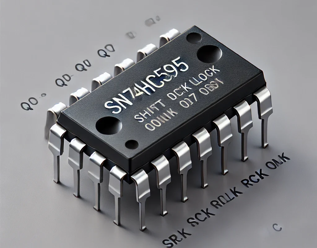
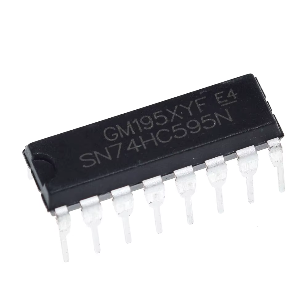
The SN74HC595 is an 8-bit serial-in, parallel-out shift register with a storage register and tri-state outputs. It is widely used for expanding the number of digital output pins on a microcontroller (e.g., Arduino, Raspberry Pi, STM32) when the available pins are limited.
🔹 1. What is the SN74HC595?
- It is an 8-bit shift register that takes serial data (one bit at a time) and outputs it in parallel (to 8 output pins).
- It includes a latch function, which holds the data until it is updated.
- The tri-state output allows multiple shift registers to be cascaded.
📌 Why use it?
- Expands microcontroller output pins (uses only 3 control pins to control 8 outputs).
- Can cascade multiple SN74HC595s to control more outputs.
- Commonly used for LED displays, 7-segment displays, and multiplexing applications.
🔹 2. SN74HC595 Pinout & Functions
The SN74HC595 has 16 pins.
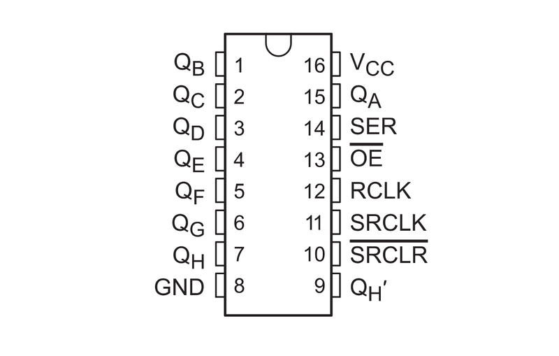
| Pin No. | Name | Function |
|---|---|---|
| 1 | Q1 | Parallel Output 1 |
| 2 | Q2 | Parallel Output 2 |
| 3 | Q3 | Parallel Output 3 |
| 4 | Q4 | Parallel Output 4 |
| 5 | Q5 | Parallel Output 5 |
| 6 | Q6 | Parallel Output 6 |
| 7 | Q7 | Parallel Output 7 |
| 8 | GND | Ground |
| 9 | Q7′ | Serial Out (for cascading) |
| 10 | MR | Master Reset (Active LOW) |
| 11 | SH_CP | Shift Register Clock |
| 12 | ST_CP | Storage Register (Latch) Clock |
| 13 | OE | Output Enable (Active LOW) |
| 14 | DS | Serial Data Input |
| 15 | Q0 | Parallel Output 0 |
| 16 | VCC | Power Supply (2V – 6V) |
📌 Key Control Pins:
- SH_CP (Pin 11) → Shift register clock (loads serial data bit-by-bit).
- ST_CP (Pin 12) → Latch clock (updates all 8 outputs).
- OE (Pin 13) → Output Enable (LOW to enable, HIGH to disable outputs).
- DS (Pin 14) → Serial data input (data fed into the shift register).
- Q7′ (Pin 9) → Serial out (for cascading more shift registers).
🔹 3. How SN74HC595 Works
- Data is sent serially (bit by bit) into DS (Pin 14).
- SH_CP (Shift Clock) moves data through the shift register.
- ST_CP (Latch Clock) transfers the stored bits to the output pins (Q0-Q7).
- OE (Output Enable) controls whether the outputs are active.
📌 Multiple SN74HC595s can be cascaded by connecting Q7' (Pin 9) of one IC to DS (Pin 14) of the next.
🔹 4. Using SN74HC595 with Arduino
🛠 Required Components
- 1x SN74HC595 Shift Register
- 8x LEDs
- 8x 220Ω Resistors
- 1x Arduino Board
- Jumper Wires
🛠 Wiring
| SN74HC595 Pin | Arduino Pin | Function |
|---|---|---|
| VCC (16) | 5V | Power |
| GND (8) | GND | Ground |
| DS (14) | D2 | Serial Data Input |
| SH_CP (11) | D3 | Shift Clock |
| ST_CP (12) | D4 | Latch Clock |
| OE (13) | GND | Always Enabled (LOW) |
| MR (10) | 5V | No Reset (HIGH) |
| Q0 – Q7 | LEDs via 220Ω Resistors | Parallel Outputs |
🔹 5. Arduino Code to Control LEDs
This Arduino sketch shifts binary data into SN74HC595 to control 8 LEDs.
#define DS 2     // Data pin
#define SH_CP 3  // Shift Clock pin
#define ST_CP 4  // Latch Clock pin

void setup() {
    pinMode(DS, OUTPUT);
    pinMode(SH_CP, OUTPUT);
    pinMode(ST_CP, OUTPUT);
}

void loop() {
    for (int i = 0; i < 256; i++) {
        digitalWrite(ST_CP, LOW);  // Latch disabled
        shiftOut(DS, SH_CP, MSBFIRST, i);  // Send data
        digitalWrite(ST_CP, HIGH); // Latch enabled
        delay(500);
    }
}
📌 Explanation:
shiftOut()sends 8 bits of data serially to SN74HC595.ST_CP(Latch Clock) updates all outputs at once.- The loop cycles through 256 patterns (
0b00000000to0b11111111).
🔹 6. Cascading Multiple SN74HC595 Shift Registers
You can connect multiple SN74HC595s together to control 16, 24, or more outputs.
🛠 Cascading Wiring
| 1st SN74HC595 Pin | 2nd SN74HC595 Pin |
|---|---|
| VCC | VCC |
| GND | GND |
| DS (Pin 14) | Arduino D2 |
| SH_CP (Pin 11) | SH_CP (Pin 11) |
| ST_CP (Pin 12) | ST_CP (Pin 12) |
| Q7′ (Pin 9) | DS (Pin 14) |
📌 Data shifts from the first SN74HC595 to the second one, allowing more outputs.
✅ Arduino Code for Two SN74HC595 Shift Registers
#define DS 2
#define SH_CP 3
#define ST_CP 4

void setup() {
    pinMode(DS, OUTPUT);
    pinMode(SH_CP, OUTPUT);
    pinMode(ST_CP, OUTPUT);
}

void loop() {
    digitalWrite(ST_CP, LOW);
    shiftOut(DS, SH_CP, MSBFIRST, 0b10101010); // First register
    shiftOut(DS, SH_CP, MSBFIRST, 0b11001100); // Second register
    digitalWrite(ST_CP, HIGH);
    delay(500);
}
📌 What happens?
- The first shift register controls the first 8 outputs.
- The second shift register controls the next 8 outputs.
🔹 7. Applications of SN74HC595
✅ LED Displays – Used in multiplexed LED matrix.
✅ 7-Segment Displays – Drives multiple digits with minimal pins.
✅ Motor Controllers – Expands H-Bridge drivers.
✅ Relays & Actuators – Controls high-power devices with low pin usage.
✅ Home Automation – Expands I/O in smart control systems.
🔹 8. SN74HC595 vs. Other Shift Registers
| Feature | SN74HC595 | 74HC164 | TPIC6B595 |
|---|---|---|---|
| Bits | 8 | 8 | 8 |
| Storage Latch | Yes | No | Yes |
| Tri-State Outputs | Yes | No | Yes |
| Max Current per Pin | 35mA | 25mA | 150mA |
| Best for | LEDs, displays | Basic shifting | High-power loads |
📌 Verdict: SN74HC595 is best for general output expansion, but for high-current applications, use TPIC6B595.
🎯 Conclusion
- The SN74HC595 expands digital outputs using only 3 control pins.
- It is widely used in LED displays, multiplexing, and motor control.
- Multiple SN74HC595s can be cascaded to control dozens of outputs.
- Arduino + SN74HC595 = Simple and Effective I/O Expansion.