
Ten lights, one moving point: a CD4017 counter can make a sequence visible without a microcontroller. The useful lesson is what makes the point move. A clock edge advances it, a reset returns it to the beginning, and an inhibit input can stop it. One apparently harmless control change can also produce an extra count.
Design review, not a measured build. This is a standalone, regulated 5 V tabletop experiment. The equations and supplied computer model have local checks; component tolerances, contact bounce, startup behaviour and real waveforms still need bench measurements. No firmware is required.
Choose the actual parts
An integrated circuit (IC) contains interconnected electronic devices on one chip. Use Texas Instruments CD4017BE, 16-pin plastic dual-in-line package (PDIP), package code N, as U2. The E suffix identifies this through-hole version. Its ten decoded outputs represent positions zero through nine; the physical output pins are not in numerical sequence. CD4022B, shown beside it in the datasheet, has eight states and a different output mapping. Do not substitute it by following this drawing.
U1 is Texas Instruments TLC555CP, 8-pin PDIP, package code P. It supplies a repeating clock. This complementary metal-oxide-semiconductor (CMOS) timer is specified separately from a bipolar NE555. A similar name or pin arrangement does not establish identical supply current or output voltage. Use the named versions for this experiment.
- U1 and U2 above; breadboard and short jumper wires.
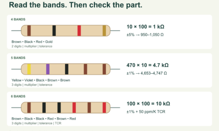
- R1: 100 kΩ; R2: 680 kΩ; R3: 10 kΩ; R4 and R5: 100 kΩ. Use 1% resistors rated at least 0.125 watts (W), a unit of power. A kilohm (kΩ) is 1,000 ohms.
- R10–R19: ten separate 22 kΩ, 1% resistors, one per light.
- C1: 1 µF film timing capacitor, ±10%, rated at least 16 V. A microfarad (µF) is one millionth of a farad. Avoid substituting a leaky electrolytic here without checking its timing effects.
- C2: 10 nF ceramic; C3 and C4: 100 nF ceramic; C5: 1 µF electrolytic, rated at least 10 V, with its positive lead at +5 V. A nanofarad (nF) is one billionth of a farad.
- D0–D9: ten high-efficiency red light-emitting diodes (LEDs). A milliampere (mA) is one thousandth of an ampere. They run dimly at roughly 0.1 mA; check visibility in your room.
- S1: normally open momentary RESET button. S2: single-pole on/off INHIBIT switch. S3: single-pole on/off CLOCK HOLD switch.
- A regulated 5.00 V direct-current supply with a 20 mA current limit for initial bring-up, and a digital voltmeter. An oscilloscope (voltage plotted against time) or logic analyser (recorded high/low states) with 5 V-compatible inputs is optional.
CD4017B has a recommended supply range of 3–18 V, but this complete circuit stays at 5 V. Its 20 V absolute maximum is a stress limit, not an operating target, and it does not apply to the TLC555. The TLC555CP commercial temperature range is 0–70°C; this lesson assumes an ordinary room-temperature bench. A current-limited supply cannot correct reversed IC power pins.
Wire the timer and counter
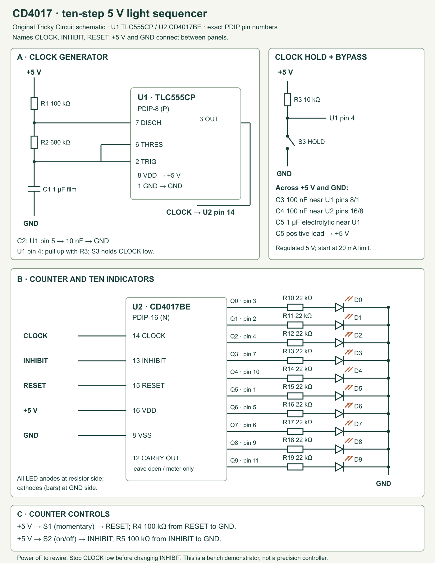
Disconnect power while wiring. A package drawing is viewed from above: place the notch upward, find pin 1 at the upper left, count down the left row and continue up the right. U1 has eight pins; U2 has sixteen. The diagram is organised by function rather than physical position. Check each numbered pin against the manufacturer’s top view before powering up.
Timer supply and control: connect U1 pin 8 to +5 V and pin 1 to the common 0 V reference, ground (GND). Put C3 between these pins and C5 across the nearby rails. Connect pin 4, the active-low timer reset, to +5 V through R3. S3 connects pin 4 to GND when closed. Closing S3 therefore holds the clock output low. Connect C2 between pin 5, the control-voltage node, and GND; do not tie pin 5 directly to a supply rail.
Timing network: connect R1 from +5 V to U1 pin 7, the discharge output. Connect R2 from pin 7 to the timing node. Join U1 pins 2 and 6 to that node and connect C1 from there to GND. Pin 2 starts a charging interval when the voltage is low enough; pin 6 ends it when the voltage is high enough. Pin 3 is the clock output and connects directly to U2 pin 14. Nothing else loads this clock node.
Counter supply: connect U2 pin 16 to +5 V and pin 8 to GND. Put C4 directly between these supply pins. These small bypass capacitors provide nearby transient current; C1 has the separate job of setting time. Verify continuity across split breadboard power rails instead of assuming their entire length is connected.
Counter controls: connect U2 pin 15, RESET, to GND through R4 and to +5 V through S1. Connect pin 13, CLOCK INHIBIT, to GND through R5 and to +5 V through S2. R4 and R5 define low levels when their switches are open. RESET is active high on U2, whereas reset is active low on U1. Confusing these polarities is a common reason for a permanently stopped display.
| Position | U2 output pin | Light branch to GND |
|---|---|---|
| Q0 | 3 | R10 → D0 anode; D0 cathode → GND |
| Q1 | 2 | R11 → D1 → GND |
| Q2 | 4 | R12 → D2 → GND |
| Q3 | 7 | R13 → D3 → GND |
| Q4 | 10 | R14 → D4 → GND |
| Q5 | 1 | R15 → D5 → GND |
| Q6 | 5 | R16 → D6 → GND |
| Q7 | 6 | R17 → D7 → GND |
| Q8 | 9 | R18 → D8 → GND |
| Q9 | 11 | R19 → D9 → GND |
Every LED branch has the same direction: output → resistor → LED anode → LED cathode → GND. The cathode is the bar side of the symbol. U2 pin 12, CARRY OUT, is an output; leave it unconnected unless measuring with a high-impedance instrument that draws little input current and accepts 5 V. Do not ground an unused output. All U1 and U2 input pins have defined connections in this design.
Predict the speed and current
In the timer’s astable mode, meaning continuous self-oscillation, C1 charges through R1 + R2 and discharges through R2. Using ideal thresholds of one third and two thirds of the supply, the steady repeating times are:
tHIGH = ln(2) × (R1 + R2) × C1 = 0.54065 s
tLOW  = ln(2) × R2 × C1        = 0.47134 s
T     = tHIGH + tLOW          = 1.01199 s
f     = 1 / T                 = 0.98815 Hz
High fraction = tHIGH / T     = 53.42%
Ten-state cycle = 10 × T      = 10.1199 s
Hertz (Hz) means cycles per second. The natural logarithm ln(2) comes from the exponential charging curve. The first charge starting at zero volts is longer: ideally ln(3) × (R1 + R2) × C1 = 0.85692 s. Starting the oscillator is therefore not the same as resuming a perfect one-second metronome.
With both timing resistors at ±1% and C1 at ±10%, the passive-component period corners are about 0.90169–1.12433 s, corresponding to roughly 1.109–0.889 Hz. This calculation excludes timer threshold errors, leakage, temperature drift and measurement loading. It is not a guaranteed accuracy specification. Measure ten complete cycles and divide by ten to reduce your stopwatch reaction error.
Assuming a 4.6 V high output and a 2.0 V red LED drop, one light draws (4.6 − 2.0)/22,000 ≈ 0.118 mA. Even the deliberately conservative resistor-only bound, 5 V / 21,780 Ω, is only 0.230 mA. The datasheet’s 5 V output-high test supports at least 0.36 mA magnitude at 4.6 V across its listed temperatures. The smaller load is intentional: these outputs are logic signals, not power drivers. A 330 Ω resistor would ask for milliamps and is outside this design’s justification.
The TLC555’s 5 V output-high specification is at least 4.1 V at a 1 mA source load; the CD4017’s high-input requirement is 3.5 V. The corresponding low specifications, at their stated test loads, are at most 0.5 V and 1.5 V respectively. Here the timer drives only a CMOS input. Do not attach a bright clock LED or a 3.3 V-only microcontroller pin and assume this interface analysis still applies.
One active output, ten positions
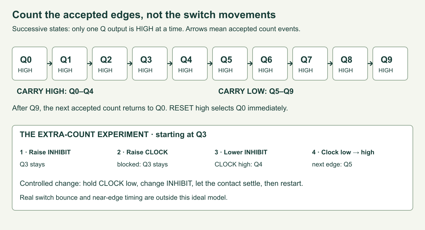
A rising edge is a change from low to high. With RESET low and INHIBIT low, a rising clock edge moves Q0 → Q1 → … → Q9 → Q0. A high output selects one light; the other outputs stay low. This is called a one-hot representation. It is not the four-bit binary number 0–9, and connecting several outputs together does not combine their meanings safely.
A high RESET immediately selects Q0, without waiting for a clock edge. It does not turn all ten lights off. Power-up is not a substitute for a deliberate reset. CARRY OUT is high during states Q0–Q4 and low during Q5–Q9, giving a full cycle for every ten accepted counts in uninterrupted operation. It is not a brief pulse that occurs only at Q9.
Three bench experiments
- Establish a known start. Close S3 to hold the timer output low, leave S2 open, and hold S1 while applying power. Check the 5 V rails. D0 should be the only selected light. Release S1 while S3 remains closed; wait at least a millisecond before starting the clock. Open S3 and watch the sequence. Ignore the first timing interval when estimating the steady frequency.
- Separate stopping from resetting. Close S3 to freeze the oscillator at low. Note which light remains selected; stopping does not force Q0. Press S1 and observe Q0. Release S1, then open S3. Next, close S3, close S2, and reopen S3. The timer runs but the selected counter output should stay fixed. A meter on the clock averages a changing signal; a middle reading does not by itself mean a bad logic level.
- Expose the inhibit trap. With the clock running and S2 closed, opening S2 while the clock is high can advance the counter immediately. Contact bounce can cause additional transitions. This is a qualitative fault experiment, not a promise of exactly one extra light on every try. To avoid this during controlled operation, close S3, change S2 while the clock is low, let the contact settle, and then reopen S3. S3 is also a mechanical switch: its contact bounce can create clock edges during stop/restart, so this manual arrangement does not guarantee an exact resume count. A precisely timed controller would need debounced, synchronised control logic, so control changes are aligned with the clock.
The reason for the trap is inside the counter’s clock gating: a falling transition on pin 13 can act as a count event when pin 14 is high. The datasheet explicitly permits pin 13 as an alternate clock under that condition, with a rise/fall-time requirement. Pin 14 has Schmitt-trigger action, meaning separate rising and falling switching thresholds, which tolerates a slowly moving input edge; this is not a guarantee that bouncing contacts produce only one edge.
At 5 V the CD4017 timing table gives minimum clock pulse width 200 ns, inhibit setup 230 ns, reset width 260 ns and reset removal 400 ns. A nanosecond (ns) is one billionth of a second. The slow oscillator leaves ample pulse width, but moving a mechanical control near an edge can still violate setup or recovery timing. The instruction to stop the clock and wait is about sequencing controls, not merely making the clock slow.
Record the measured supply, R1/R2/C1 markings, ten-cycle time, active output before/after reset, and observations when changing inhibit. If available, capture CLOCK, INHIBIT and the selected outputs together on a 5 V-compatible instrument. Keep bench results separate from calculated predictions.
Run the complete logic model
Save the following as cd4017_model.py (cd4017_model.py inside ZIP) and run python3 cd4017_model.py on a computer. It models accepted logic events and computes ideal timer values. It does not model transistor currents, propagation delay, contact bounce or analog thresholds. Inputs must already be valid logic levels. Unknown startup state remains unknown until reset; conflicting simultaneous control changes are rejected instead of assigned an invented ordering.
"""Ideal CD4017 logic and TLC555 timing calculator; NOT firmware or an analog circuit simulation.

Call apply() in chronological order after voltages have settled. Simultaneous
clock/inhibit changes are rejected because propagation ordering matters.
Unknown power-up state persists until reset. No analog bounce or delays modeled.
"""
from math import log, isfinite


def astable(ra=100_000, rb=680_000, capacitance=1e-6):
    for value in (ra, rb, capacitance):
        if isinstance(value, bool) or not isfinite(value) or value <= 0:
            raise ValueError("R and C must be finite positive numbers")
    high = log(2) * (ra + rb) * capacitance
    low = log(2) * rb * capacitance
    return {"high_s": high, "low_s": low, "period_s": high + low,
            "frequency_hz": 1 / (high + low), "high_fraction": high / (high + low),
            "first_high_from_zero_s": log(3) * (ra + rb) * capacitance}


class Counter4017:
    """One-hot ten-state counter; None means startup state not established."""
    def __init__(self):
        self.state = None
        self.clock = False
        self.inhibit = False
        self.reset = False

    def apply(self, *, clock=None, inhibit=None, reset=None):
        values = [self.clock if clock is None else clock,
                  self.inhibit if inhibit is None else inhibit,
                  self.reset if reset is None else reset]
        if any(type(v) is not bool for v in values):
            raise ValueError("Inputs must be bool, or omitted")
        clk, inh, rst = values
        if not rst and clk != self.clock and inh != self.inhibit:
            raise ValueError("Change clock and inhibit separately; timing is undefined here")
        if not rst and self.reset and (clk != self.clock or inh != self.inhibit):
            raise ValueError("Release reset separately; observe real recovery time")
        rising_clock = not self.clock and clk and not inh
        falling_inhibit = self.inhibit and not inh and clk
        if rst:
            self.state = 0
        elif rising_clock or falling_inhibit:
            if self.state is not None:
                self.state = (self.state + 1) % 10
        self.clock, self.inhibit, self.reset = clk, inh, rst
        return self.snapshot()

    def snapshot(self):
        return {"state": self.state,
                "outputs": None if self.state is None else
                [int(i == self.state) for i in range(10)],
                "carry": None if self.state is None else int(self.state < 5)}


if __name__ == "__main__":
    print("Calculated timing, not measured:", astable())
    counter = Counter4017()
    print("Before reset:", counter.snapshot())
    counter.apply(reset=True)
    counter.apply(reset=False)
    for _ in range(12):
        print(counter.apply(clock=True))
        counter.apply(clock=False)
    counter.apply(inhibit=True)       # CLOCK is LOW: stop safely
    counter.apply(clock=True)         # blocked clock edge
    print("Paused:", counter.snapshot())
    print("Inhibit released HIGH:", counter.apply(inhibit=False))
Diagnose what the display is telling you
- Only D0 stays on: check that U2 RESET is low after releasing S1, INHIBIT is low, U1 reset is high, and clock pin 14 is connected to U1 pin 3.
- The sequence jumps in physical order: inspect the output-pin table. Q4 is pin 10, whereas Q5 is pin 1. Arrange lights by Q number, not package position.
- One position looks blank: turn power off and inspect that LED’s orientation and its resistor. Do not lower all resistor values to compensate for a reversed light.
- Several lights remain steadily bright: check bridges between output rows and incorrect power connections. Disconnect power before probing continuity.
- Speed varies substantially: measure the timing parts, inspect C1 leakage and clean the breadboard. A meter across the timing node adds resistance and capacitance; compare the speed with and without it.
- Restart changes the selected position: repeat the deliberate reset sequence. The model intentionally does not promise a particular power-up state.
Do not use this demonstration as a safety interlock, accurate clock or motor sequencer. Motors and relays need suitable drivers, supply design and protection; the ten indicator outputs are not rated to power them. A four-step version that ties Q4 directly to RESET also needs a separate timing analysis of the self-generated reset pulse. A brief simulation is not enough to establish reliable reset pulse width.
Challenge: predict the hidden edge
Start in Q3 with CLOCK low and INHIBIT low. Raise INHIBIT, raise CLOCK, lower INHIBIT while CLOCK is still high, lower CLOCK, then raise CLOCK. Which light is selected at the end? What happens if RESET is held high throughout?
Show the reasoning
Raising INHIBIT does not count. The following rising clock is blocked, so Q3 remains. Lowering INHIBIT while CLOCK is high advances to Q4. The falling clock does not count. The last rising clock advances to Q5. With RESET held high, Q0 remains selected throughout. Try the same sequence through Counter4017.apply(); a physical switch can bounce and must not be treated as one ideal transition.
Sources and further experiments
The reviewed sources are TI CD4017B/CD4022B datasheet SCHS027C (technical revision February 2004; current package addendum September 2026), the exact CD4017BE orderable package, and TI TLC555 datasheet SLFS043K, January 2026. Product documentation pages were checked on 12 October 2026; no separate errata document was found there. Recheck the manufacturer pages before selecting another suffix or revising the circuit.
Practice measuring a resistor’s voltage with the 5 V LED-current experiment, and explore changing signals in the electronics laboratory. This sequencer’s distinct lesson is the difference between an intended control action and the electrical edge that a chip actually counts.
Download the source package (ZIP): complete programs, full-size PNG and editable SVG diagrams, and the logger’s host tests. The same complete article program is included above.