
A frequency that a loop can follow after it has settled is not necessarily one it can acquire from an unrelated starting state. The CD4046B makes that distinction visible with a voltage-controlled oscillator, two different phase comparators and an external capacitor that remembers the recent control voltage. This is a manual bench experiment, not a frequency counter or a missing-pulse detector.
Use the exact Texas Instruments (TI) CD4046BE in the N plastic dual-in-line package (PDIP), with 16 pins and a regulated, measured 5.00 volt (V) supply. A phase-locked loop (PLL) compares a reference with its own output and feeds the difference back to a voltage-controlled oscillator (VCO). A low-pass filter (LPF) smooths the comparator output. Phase comparator I (PC I) is an exclusive-OR (XOR) network; phase comparator II (PC II) uses an edge-controlled memory network. These names refer to different circuits inside the same integrated circuit (IC), not interchangeable firmware modes.
No microcontroller or firmware is needed. The supplied Python program is a host-only calculator for ideal XOR averages and a resistor-capacitor (RC) filter. It is not a physical PLL simulator. The circuit, plots and numerical examples have not been measured on hardware. They do not establish capture bandwidth, lock performance or a production timing specification.
1. Separate acquisition from tracking
First place the loop in a declared initial condition, apply a reference and ask whether its frequency and phase settle into a stable relationship. That is an acquisition trial. In a separate trial, begin with an already established relationship and move the reference slowly while watching whether that relationship persists. That is tracking. A frequency-only display cannot prove either result: two signals can have nearly equal average frequency while their relative phase keeps slipping.
The TI data sheet states that PC I’s capture range depends on the external filter and is no larger than its lock range. A loop can therefore retain a relationship at a frequency that it would not acquire from your chosen cold-start condition. That is the central comparison. Do not turn it into a rule for every comparator: the manufacturer’s ideal description of PC II gives capture range equal to lock range over the VCO range. Practical observation still depends on the completed circuit, input edges, loading and the time you allow.
PC I also can lock near harmonics, so simply observing a steady waveform is insufficient. Compare the actual reference and VCO frequencies and inspect relative phase. PC II responds to positive edges and does not have the same duty-cycle requirement or harmonic behavior. Changing comparator does not remove the need for a valid reference signal, a qualified supply and an observation window.
2. Build one explicit analog loop
All power symbols marked +5 V are one regulated source. Every ground symbol is the same return shared with the generator and oscilloscope. The IC’s VDD supply is pin 16 and VSS return is pin 8. Put C3, 100 nanofarads (nF), directly between those terminals. The loop is operated at 5 V, inside the data sheet’s recommended PLL supply range of 5–18 V. The larger absolute-maximum ratings are stress limits, not alternative operating points.
Resistance is measured in ohms (Ω). R1 is a 100 kilohm (kΩ) resistor from pin 11 to ground. Pin 12, the optional R2 timing-resistor connection, is intentionally not connected (NC), giving the no-offset configuration. CT is a 470 picofarad (pF) film timing capacitor between pins 6 and 7; it is not a bypass capacitor to ground. Inhibit pin 5 is tied LOW to ground. VCO output pin 4 feeds comparator input pin 3 directly, without a divider.
S1 is one pole with three mutually exclusive throws: manual potentiometer wiper, PC I output pin 2, or PC II output pin 13. It must break the previous connection before making the next. Its common terminal feeds RF, 100 kΩ, then VCO-control pin 9. CF, 100 nF, connects that control node to ground. S2 is a normally open discharge button through RR, 1 kΩ, to ground. That resistor avoids shorting an actively driven comparator output through a charged node. It does not force the control node to mathematically zero volts.
P1 is a Bourns 3386P-1-103LF, 10 kΩ potentiometer. Pin 3, the clockwise (CW) end, connects to +5 V; pin 1, the counterclockwise (CCW) end, connects to ground; pin 2 is the wiper and only the manual selector input. Verify the P-style footprint rather than assuming another 3386 style has the same physical pin placement. Its ceramic-and-metal, or cermet, resistive element and tolerance do not turn knob position into a calibrated voltage source.
High-impedance (Hi-Z) instrument inputs draw little current from the observed node; their remaining resistance and capacitance still load it.
Unused pin 10 is the demodulator source-follower output, which follows the control voltage with an offset under its required load. Pin 15 connects to the optional zener diode, a voltage-limiting element kept open here because the supply is already regulated.
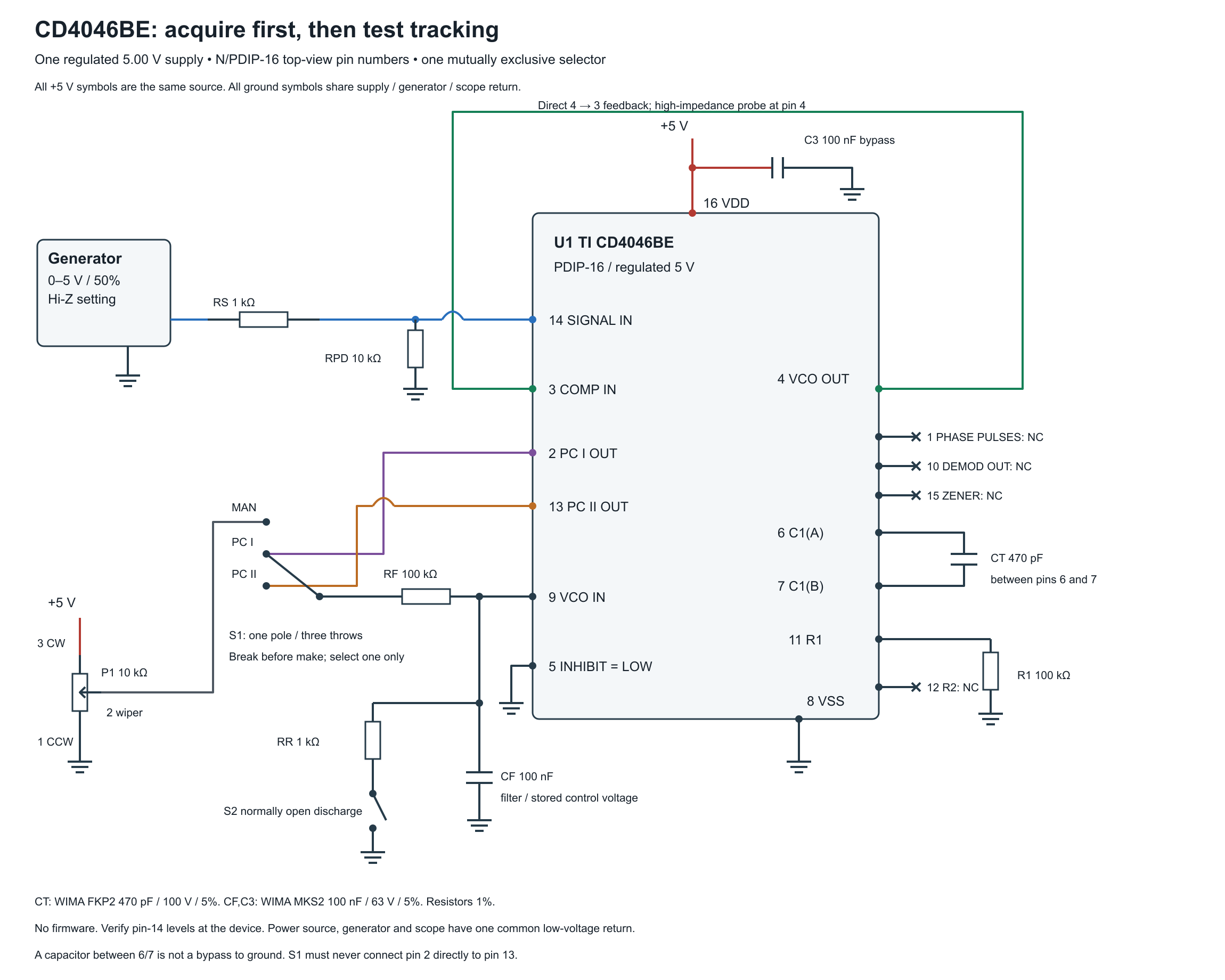
| CD4046BE terminal | Connection and role |
|---|---|
| 16 / 8 | One +5 V supply / common ground; C3 bypass between them |
| 14 SIGNAL IN | Generator through RS 1 kΩ; RPD 10 kΩ to ground |
| 4 VCO OUT / 3 COMP IN | Direct feedback; high-impedance scope input at pin 4 |
| 2 PC I / 13 PC II | Separate selector throws; never tied directly together |
| 9 VCO IN | RF output, CF to ground and S2/RR discharge branch |
| 6 / 7 | CT 470 pF between the two timing terminals |
| 11 / 12 | R1 100 kΩ to ground / R2 port intentionally open |
| 5 | Inhibit tied to ground, enabling VCO |
| 1 / 10 / 15 | Phase-pulse output / demodulator source-follower output / optional zener terminal unused, all open |
Use 1% metal-film resistors, such as Vishay MRS25 parts at the stated values. CT is WIMA FKP2D004701D00JSSD, 470 pF, 100 V, 5%; CF and C3 are WIMA MKS2C031001A00JSSD, 100 nF, 63 V, 5%. These higher capacitor voltage ratings do not increase the IC’s allowed input or supply voltage. The filter and oscillator capacitors have different jobs and must not be exchanged merely because both are called timing components.
3. Qualify the generator and probes
The reference generator is the sole active source on pin 14. Configure a square wave with 50% duty cycle and a nominal 0–5 V output using its high-impedance load setting. Measure the actual waveform at pin 14, after RS and RPD. A generator display configured for a 50 Ω load can give a different open-circuit amplitude; do not connect it based only on the display. The reference and VCO comparison inputs need LOW at or below 30% of the supply and HIGH at or above 70%, corresponding to 1.5 V and 3.5 V at 5 V.
The nominal RS/RPD divider would give 5 × 10/11 = 4.545 V HIGH before the generator’s output resistance and IC input loading. Its LOW branch also gives a defined return when the source is disconnected, but verify that LOW at the actual input rather than relying on an assumed internal bias. Do not use a low-amplitude logic output that cannot meet the required HIGH. RS is not a complete overvoltage or unpowered-input protection circuit.
Use high-impedance probes on pins 14, 4 and 9. A 10 megohm (MΩ) probe on the control node still loads RF and adds capacitance. The unloaded 100 kΩ/100 nF arithmetic below does not include that probe, switch leakage, breadboard contamination or comparator output resistance. Pin 10’s source follower is unused; do not attach a load there without the manufacturer’s required external return resistor. Pin 1 is not used as a stand-alone lock indicator.
Power the IC before applying a reference and set the generator LOW or disconnect its signal before removing IC power. Keep every input between ground and the live supply. An independent powered signal connected to an unpowered IC can inject current; the absolute-maximum input-current entry does not qualify that sequence. Change selector wiring only with power removed and the filter discharged. Verify S1 continuity in every position before installation.
4. Calculate what the simple filter does
For two ideal, equal-frequency, 50% duty square waves, the XOR output’s mean between zero and 180 degrees is VDD multiplied by phase difference divided by 180 degrees. At a 90-degree difference the mean is half the supply, 2.5 V here. This relationship explains PC I’s nominal center-frequency phase offset. It is not a rule that every 2.5 V control-node reading proves lock: an unlocked or missing-reference condition can also yield a similar average.
ideal_XOR_mean = VDD * phase_degrees / 180    # 0..180 degrees only
unloaded_tau = RF * CF = 100000 * 100e-9 = 0.010 s
unloaded_pole = 1 / (2*pi*tau) = 15.9155 Hz
ideal_step_V(t) = target + (initial-target) * exp(-t/tau)
Here seconds (s), milliseconds (ms) and hertz (Hz, cycles per second) describe the calculator’s time and frequency units. A 0-to-5 V ideal step reaches 90% of its final value after tau × ln(10), about 23.03 ms. With the entered 1% RF and 5% CF tolerances, the nominal component-corner time constants span 9.405–10.605 ms. These are not PLL settling-time or capture-time limits. In a real loop the comparator output is not simply a fixed step source.
The oscillator needs a separate voltage-to-frequency map. The application report’s illustrative 5 V design uses R1 = 100 kΩ and a 500 pF capacitor for an approximately 10 kHz center. Our available 470 pF part is close in scale, not an exact reproduction of that example. Measure your actual VCO at the control terminal voltages listed in the procedure. Do not infer a guaranteed center, linearity or capture bandwidth from a typical chart or a capacitor-value ratio.
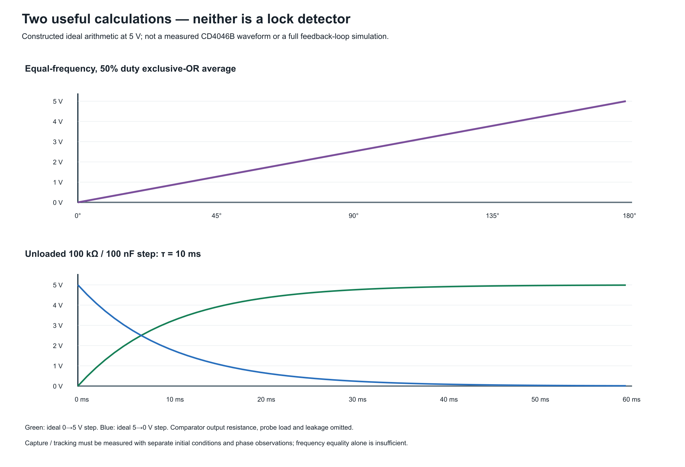
The green and blue exponential curves are only unloaded filter arithmetic. The upper line is the ideal XOR average for equal-frequency inputs. No trace is labeled as a measured loop response. PC II’s three-state output introduces another important difference: near its ideal stable operating point both output drivers can be off and the filter retains charge, subject to real leakage and loading. With no input reference, the manufacturer describes PC II driving the VCO toward its lowest frequency; PC I tends toward its center-frequency condition instead. Neither is a missing-reference safety function.
5. Use the complete host calculator
Save the file below as pll_filter_lab.py on a computer with Python 3. Run python pll_filter_lab.py for the component calculations or python pll_filter_lab.py --trace for the constructed plot rows. It has no hardware interface, no external runtime dependency and no firmware upload step. The optional observation helper only evaluates operator-entered frequency, bounded-phase and cycle-count evidence; it cannot independently verify a scope trace.
"""HOST ONLY: ideal XOR average and unloaded one-pole RC arithmetic.
Not a CD4046B/VCO/capture-range/lock simulation; no firmware or GPIO.
"""
import math,json,argparse

def finite(v):
    if isinstance(v,bool)or not isinstance(v,(int,float))or not math.isfinite(v):raise ValueError('FINITE')
    return float(v)

def parameters(vdd=5.0,resistance=100000,capacitance=100e-9):
    v,r,c=map(finite,(vdd,resistance,capacitance))
    if not 5<=v<=5.25 or not 10000<=r<=1000000 or not 100e-12<=c<=1e-6:raise ValueError('LESSON_DOMAIN')
    return v,r,c

def xor_average(phase_degrees,vdd=5.0):
    v,_,_=parameters(vdd);p=finite(phase_degrees)
    if not 0<=p<=360:raise ValueError('PHASE')
    return v*min(p,360-p)/180 # equal-frequency,50%duty,ideal rail-to-rail signals

def filter_step(t_s,initial_V,target_V,resistance=100000,capacitance=100e-9,vdd=5.0):
    v,r,c=parameters(vdd,resistance,capacitance);t,a,b=map(finite,(t_s,initial_V,target_V))
    if not 0<=t<=10 or not 0<=a<=v or not 0<=b<=v:raise ValueError('STEP_DOMAIN')
    return b+(a-b)*math.exp(-t/(r*c))

def corners(resistance=100000,capacitance=100e-9,r_fraction=.01,c_fraction=.05):
    _,r,c=parameters(5,resistance,capacitance);er,ec=map(finite,(r_fraction,c_fraction))
    if not 0<=er<=.1 or not 0<=ec<=.2:raise ValueError('TOLERANCE')
    lo=r*(1-er)*c*(1-ec);hi=r*(1+er)*c*(1+ec)
    return{'nominal_tau_s':r*c,'tau_min_s':lo,'tau_max_s':hi,
           'nominal_pole_Hz':1/(2*math.pi*r*c),'pole_min_Hz':1/(2*math.pi*hi),
           'pole_max_Hz':1/(2*math.pi*lo),'nominal_t90_s':math.log(10)*r*c,
           'scope':'Entered component tolerances only; no output resistance,probe,leakage or PLL capture bounds'}

def compatible_observation(reference_Hz,vco_Hz,phase_bounded,cycles,relative_tolerance=.001):
    f,g,e=map(finite,(reference_Hz,vco_Hz,relative_tolerance))
    if not 1<=f<=100000 or not 1<=g<=100000 or not 0<e<=.01:raise ValueError('OBSERVATION_DOMAIN')
    if type(phase_bounded)is not bool or type(cycles)is not int or not 10<=cycles<=100000:raise ValueError('OBSERVATION_EVIDENCE')
    return{'assessment':'LOCK_COMPATIBLE_OBSERVATION'if phase_bounded and abs(f-g)/f<=e else'LOCK_NOT_ESTABLISHED',
           'relative_frequency_error':abs(f-g)/f,'cycles_observed':cycles,
           'scope':'Operator-entered finite window; no future lock,correct harmonic,or independent verification'}

def trace():
    return{'state':'CONSTRUCTED_ARITHMETIC','corners':corners(),
           'phase_rows':[{'degrees':p,'mean_V':xor_average(p)}for p in range(0,181,5)],
           'step_rows':[{'time_s':i*.001,'rising_V':filter_step(i*.001,0,5),
                         'falling_V':filter_step(i*.001,5,0)}for i in range(61)],
           'physical_measurements':None,'capture_range_Hz':None,'VCO_frequency_model':None}

def main():
    p=argparse.ArgumentParser(description=__doc__);p.add_argument('--trace',action='store_true');a=p.parse_args()
    print(json.dumps(trace()if a.trace else corners(),indent=2))
if __name__=='__main__':main()
All inputs must be finite and inside the lesson’s declared domain. Boolean values are not accepted as numeric measurements. The time domain is deliberately finite, so an enormous floating-point time does not masquerade as a useful experiment. Invalid values raise instead of turning into zero frequency, successful lock or an extrapolated capture range. The output leaves capture_range_Hz and VCO_frequency_model null.
6. Compare two initial conditions at the same reference
- With power removed, verify the notch orientation, all 16 terminal assignments, CT between 6/7, separate comparator outputs, common returns and S1’s exclusive positions. Confirm that no input is left unintentionally floating.
- Select manual control. Power the 5 V rail with an appropriate current limit. Keep the generator LOW. Set P1 so measured pin 9 is successively about 0.5, 1.5, 2.5, 3.5 and 4.5 V. Wait for the filter and record the actual VCO frequency and waveform at each point. Do not replace measured control voltage with knob markings.
- Remove power, discharge CF and select PC I. Set a reference near the measured center-frequency region. Power up, verify pin-14 levels and duty cycle, and observe both reference and VCO. Allow a declared observation interval, such as two seconds, then record frequency agreement and relative phase over at least 100 cycles. A continuing phase walk means lock has not been established.
- For a capture trial, hold S2 until pin 9 is measured near its low-control condition, then release it with the chosen reference present. Record the initial control voltage, reference frequency, observation duration and whether phase became bounded. Repeat from the same initial condition. The discharge resistor means the held node may be a few tens of millivolts, not exact zero.
- For tracking, first establish a bounded relationship near the center. Move the reference in small steps while observing phase continuously. Record the last qualified point and the first failure in each direction. The result is tied to step size, dwell, input waveform and your completed circuit, not a universal IC bandwidth.
- Choose a reference near an observed tracking boundary. Compare a fresh low-control capture trial with an already-tracking approach to that same reference. A different outcome illustrates path dependence without requiring a fabricated numeric capture specification.
- Power down, discharge and select PC II. Repeat the defined procedure. Do not expect the PC I inequality to prove a narrower PC II capture range. Compare its control-node storage, phase behavior and response when the generator is forced LOW. Restore a valid reference before making another lock observation.
Pressing S2 while a comparator is HIGH creates a nominal 5/(100000+1000) = 49.5 microampere (µA) path and about 0.0495 V at the discharged control node, ignoring output resistance. It is a repeatable low-control request, not a reset input that forces every internal comparator state. Record the actual voltage and release conditions. A high-impedance node may drift when no driver is on; do not call retained capacitor voltage proof that the reference is still present.
The blank worksheet records separate capture and tracking rows, comparator, initial control voltage, reference/VCO frequency, phase observation, number of cycles, dwell and probe loading. No physical rows are supplied. The host checks cover the actual equations, tolerance corners, input domains, ideal step identities and the requirement that frequency equality alone is insufficient. They do not validate the CD4046B’s analog loop or a target firmware binary.
7. Challenge
A frequency counter shows 5000 Hz on both pin 14 and pin 4, but the relative phase repeatedly walks through a full cycle. Has the loop acquired lock? Could a steady 2.5 V at pin 9 settle the question?
Show the answer
No. Equal average frequency is insufficient when phase keeps slipping. A 2.5 V average can occur without a qualified locked relationship, particularly with PC I’s averaging behavior. Inspect the two waveforms over a declared finite window, check the intended frequency ratio and retain the initial-state and filter conditions. The capacitor stores voltage; it does not store evidence that the reference remains valid.
8. Downloads and primary references
Download the compressed ZIP archive with calculator, checks, blank worksheet and original diagrams (ZIP; file: tricky-circuit-campaigns99-104/batch-011/packages/cd4046b-capture-versus-lock/experiment-tests.zip), complete host calculator (ZIP; file: tricky-circuit-campaigns99-104/batch-011/packages/cd4046b-capture-versus-lock/pll_filter_lab.py), blank observations worksheet (ZIP; file: tricky-circuit-campaigns99-104/batch-011/packages/cd4046b-capture-versus-lock/observations-blank.csv), and editable functional circuit (ZIP; file: tricky-circuit-campaigns99-104/batch-011/packages/cd4046b-capture-versus-lock/pll-functional.svg) / arithmetic graph (ZIP; file: tricky-circuit-campaigns99-104/batch-011/packages/cd4046b-capture-versus-lock/pll-arithmetic.svg). Scalable Vector Graphics (SVG) files remain editable; Portable Network Graphics (PNG) originals open through the figure links.
For background, see the electronics course and low-pass filter lesson. Primary sources: TI CD4046B SCHS043B, revised July 2003, with current package addendum; TI SCHA002A application report; exact CD4046BE orderable and N package; WIMA FKP2 timing capacitor; WIMA MKS2 filter and bypass capacitor; Bourns 3386 P-style pin map; and Vishay MRS25 resistors. The older application report includes different general rating summaries; the exact current-linked data sheet governs this 5 V fixture. No absence-of-all-errata claim or measured loop qualification is implied.
Download the complete reader files (ZIP): full programs, blank observation worksheets, original editable SVG/PNG diagrams and selected support files for cd4046b-capture-versus-lock. Inline main programs remain complete; this download is supplementary.