Integrated circuits · serial nonvolatile memory
Make three write attempts to the same scratch byte. Enable the first, skip the enable command for the second, then enable the third. Read both the permission bit and the stored byte to find out which writes took effect.
One byte, two things to observe
Serial Peripheral Interface (SPI) uses a shared clock and separate input and output wires to move bits between a controller and a peripheral. Here the controller is an original Raspberry Pi Pico and the peripheral is an Infineon FM25V02A-G. It is ferroelectric random-access memory (F-RAM), which retains stored bytes when power is removed. Its 256-kilobit array holds 32,768 eight-bit bytes.
The write-enable latch (WEL) is a one-bit permission flag inside the device. An SPI command named Write Enable (WREN) sets it. Reading the status register reveals the flag, while reading the scratch address reveals the actual stored byte. The status and data answer different questions. Compare with the two-record settings store built around a different serial memory. 24LC256 settings store experiment
Wire the dedicated scratch fixture
Use an original non-wireless Pico with the RP2040 microcontroller, one FM25V02A-G, a plain 2.54 mm adapter, short jumpers, a 4.7 kΩ ±1% resistor, two 47 kΩ ±5% resistors and one 100 nF ceramic capacitor rated at least 6.3 V. The -G orderable comes in an eight-pin small-outline integrated-circuit (SOIC-8) package. Orient it by the pin-one mark in the top view. GP labels identify the Pico’s general-purpose input/output (GPIO) pins. Use a device dedicated to this exercise because the test leaves a new value at address 0x1234.
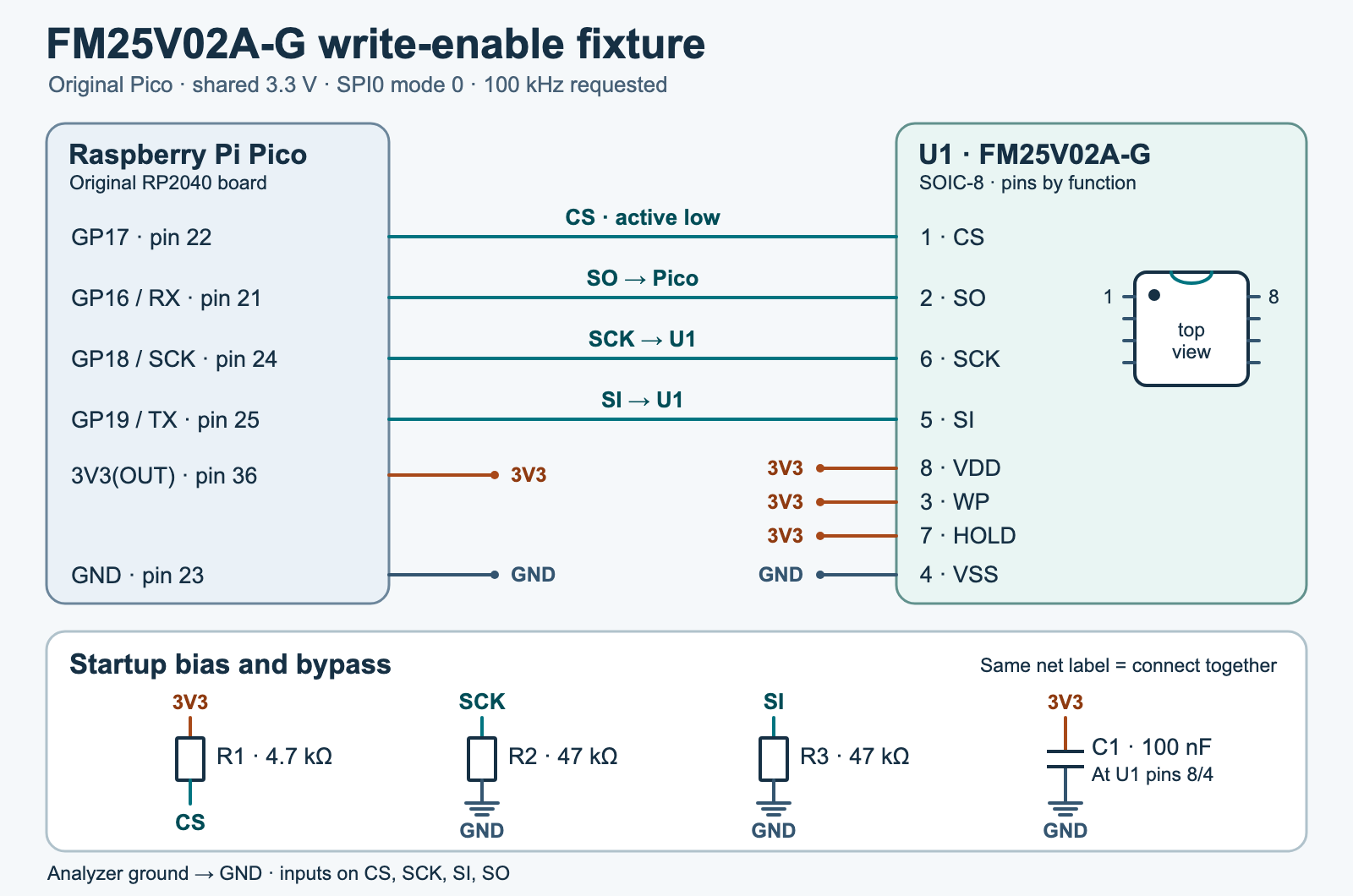
fixture.svg)Chip select (CS) is active low, so a low level selects the memory. Serial output (SO) goes to the Pico receive pin (RX). Serial input (SI) receives data from the Pico transmit pin (TX). Serial clock (SCK) times these transfers. WP means write protect. HOLD can pause a selected transfer. VDD is the positive supply, and VSS is the ground return.
| Memory pin | Connection | Local branch |
|---|---|---|
| 1 · CS | GP17, Pico pin 22 | R1, 4.7 kΩ to 3.3 V |
| 2 · SO | GP16, Pico pin 21, receive | Optional analyzer input |
| 3 · WP | 3.3 V rail | Held high |
| 4 · VSS | Pico ground, pin 23 | C1 ground, analyzer ground |
| 5 · SI | GP19, Pico pin 25, transmit | R3, 47 kΩ to ground |
| 6 · SCK | GP18, Pico pin 24 | R2, 47 kΩ to ground |
| 7 · HOLD | 3.3 V rail | Held high |
| 8 · VDD | Pico 3V3(OUT), pin 36 | C1, 100 nF to pin 4 |
Power the Pico by Universal Serial Bus (USB) and feed the memory from the Pico’s regulated 3.3 V output. Keep the Pico’s VBUS and VSYS pins out of the memory wiring. Install C1 close to memory pins 8 and 4 to supply short current pulses locally. R1 keeps CS high during startup. R2 and R3 give the clock and data inputs a defined low level while the Pico pins are inputs. At 3.3 V the Pico sinks about 0.70 mA through R1 while CS is low. Each 47 kΩ resistor draws about 70 µA while its signal is driven high.
The memory operates from 2.0 to 3.6 V. At a 3.3 V supply, the datasheet guarantees a logic high from 2.31 V up and a logic low through 0.99 V, within the specified input ranges. The logic level between these bounds is unspecified. The datasheet’s 4.5 V absolute supply maximum is a stress limit. Use 3.3 V instruments with high-impedance inputs. Use only ground-referenced analyzer or oscilloscope inputs on the fixture and connect their ground to the shared ground. Keep leads short and connect one input per signal during the capture. Infineon datasheet, printed pages 13–17
Predict the three attempts
SPI mode 0 keeps the clock low before CS falls. The memory samples SI on rising clock edges. The program sends the most significant bit first and requests 100 kHz, giving a nominal 10 µs clock period. One write frame contains an opcode (command byte), two address bytes and one data byte. Its 32 clocks take about 320 µs at the requested rate, before software gaps. The device uses a 15-bit address. For 0x1234, send 12 34 with the high byte first and its unused top bit clear.
WREN is 06, Read Status Register (RDSR) is 05, WRITE is 02, and READ is 03. Each command gets a fresh falling CS edge. Raise CS after WREN and again after each WRITE. That final rising edge ends the write frame and clears WEL. F-RAM writes the accepted byte as it arrives, so an ordinary read can follow without a programming-delay loop. The closing edge marks the transaction boundary.
Status bit 1 is WEL. Status bits 3 and 2 are the block-protect bits (BP1 and BP0). The pair 00 protects no array addresses, 01 protects 0x6000–0x7FFF, 10 protects 0x4000–0x7FFF, and 11 protects the entire array. The scratch byte is below both upper-range boundaries. The program aborts on full protection without changing the status register. The WP pin blocks writes to the status register only when the Write Protect Enable (WPEN) bit is 1 and the WP pin is held low. A permitted status-register write still requires WEL to be set. The array permission observed here comes from WEL and the block-protect bits.
Let A be the original byte. The program computes B by exclusive OR with 0x55 and C by exclusive OR with 0xAA. Exclusive OR flips bits where the mask has a 1. Both bytes differ from A and from each other, so a matching initial value cannot disguise an ignored write.
| Step | WEL expected | Readback expected |
|---|---|---|
| Cold power-up | 0 | A |
| WREN, then read status | 1 | |
| WRITE B | 0 | B |
| WRITE C without WREN | 0 | B |
| WREN again, then read status | 1 | |
| WRITE C | 0 | C |
Run and record the experiment
- Check before power. Verify pin-one orientation and continuity from the Pico to each memory terminal. Check for shorts between power and ground or between adjacent pins. Attach the scope ground to VSS and measure VDD at the chip.
- Check the rail and CS. Keep the code off the Pico’s automatic boot path. With the fixture idle, check the VDD waveform for the specified rise and fall times per volt. The datasheet gives at least 50 µs/V on rise and 100 µs/V on fall. Record the fastest part of each edge and proceed only on a compliant supply. Verify that CS stays inactive during startup and that at least 250 µs passes from VDD reaching 2.0 V to the first falling CS edge. The program waits an additional 1 ms before starting SPI commands. A delay cannot repair an out-of-spec supply ramp.
- Arm the analyzer if available. Connect inputs to CS, SCK, SI and SO and trigger on CS falling. Use 3.3 V logic thresholds and at least 2 million samples per second for the 100 kHz decode. The first frame is a read-only device ID (RDID) check, followed by the starting status and scratch byte. Capture the complete run. For each WRITE, record the command bytes, separate CS boundary, following status and subsequent READ result.
- Save the observations. In MicroPython’s read–evaluate–print loop (REPL), import
runand evaluaterun(confirm_scratch=True). Read the six raw status bytes and four readbacks in table order. Use the blank bench worksheet (ZIP:observations-blank.csv) and enter your own readings. If a guard stops the program, save the failure and disconnect power with CS high before changing any wire. Restart from a compliant cold power-up after correcting the cause.
A wrong or all-zero device ID points to the device selection, clock mode, supply, SI/SO routing or HOLD level. Confirm the published nine-byte response for this part before writing. If WEL stays clear after WREN, look for the separate CS-high interval and verify the decoded 06 byte. If WEL sets but the first readback is wrong, check the block-protect bits and both address bytes. If the supposedly ignored write changes memory, inspect the trace for an extra WREN or a second controller.
Complete Pico program
Use MicroPython v1.29.0 for the original Pico. Save the program as fm25v02a_wel.py and copy it to the board without naming it main.py. Every command sends and receives through the same clocked transfer. For status, the second byte contains the result. For ordinary memory reads, the fourth byte contains the result after the opcode and two address bytes. The program releases CS on a software transfer error. It reports successful readback only after all three attempts agree with the prediction.
"""Read and exercise the write-enable latch on a dedicated FM25V02A-G."""

SCRATCH = 0x1234
DEVICE_ID = b"\x7f\x7f\x7f\x7f\x7f\x7f\xc2\x22\x08"
WEL = 0x02
BLOCK_PROTECT = 0x0C
RESERVED_STATUS = 0x71
CS_DELAY_US = 2


class Fram:
    def __init__(self, spi, cs, delay_us):
        self.spi = spi
        self.cs = cs
        self.delay_us = delay_us

    def exchange(self, frame):
        received = bytearray(len(frame))
        self.delay_us(CS_DELAY_US)
        self.cs(0)
        try:
            self.delay_us(CS_DELAY_US)
            self.spi.write_readinto(frame, received)
            self.delay_us(CS_DELAY_US)
        finally:
            self.cs(1)
        return received

    def status(self):
        value = self.exchange(b"\x05\x00")[1]
        if value & RESERVED_STATUS:
            raise RuntimeError("Unexpected reserved status bits: 0x%02X" % value)
        return value

    def read_scratch(self):
        frame = bytes((0x03, SCRATCH >> 8, SCRATCH & 0xFF, 0))
        return self.exchange(frame)[3]

    def write_scratch(self, value):
        frame = bytes((0x02, SCRATCH >> 8, SCRATCH & 0xFF, value))
        self.exchange(frame)


def expect_latch(status, enabled, step):
    if bool(status & WEL) != enabled:
        raise RuntimeError("%s: unexpected WEL in status 0x%02X" % (step, status))


def expect_byte(actual, expected, step):
    if actual != expected:
        raise RuntimeError(
            "%s: expected 0x%02X, read 0x%02X" % (step, expected, actual)
        )


def experiment(spi, cs, delay_us):
    """Run after a cold power-up on a device reserved for this experiment."""
    fram = Fram(spi, cs, delay_us)
    identity = bytes(fram.exchange(b"\x9f" + b"\x00" * 9)[1:])
    if identity != DEVICE_ID:
        raise RuntimeError("Unexpected FM25V02A device identity: %s" % identity)

    initial_status = fram.status()
    expect_latch(initial_status, False, "Cold power-up")
    if initial_status & BLOCK_PROTECT == BLOCK_PROTECT:
        raise RuntimeError("Block protection covers the whole array")

    initial = fram.read_scratch()
    first = initial ^ 0x55
    second = initial ^ 0xAA

    fram.exchange(b"\x06")
    enabled = fram.status()
    expect_latch(enabled, True, "First WREN")
    fram.write_scratch(first)
    written = fram.status()
    expect_latch(written, False, "First WRITE")
    read_first = fram.read_scratch()
    expect_byte(read_first, first, "First WRITE readback")

    fram.write_scratch(second)
    ignored = fram.status()
    expect_latch(ignored, False, "WRITE without WREN")
    read_ignored = fram.read_scratch()
    expect_byte(read_ignored, first, "WRITE without WREN readback")

    fram.exchange(b"\x06")
    reenabled = fram.status()
    expect_latch(reenabled, True, "Second WREN")
    fram.write_scratch(second)
    rewritten = fram.status()
    expect_latch(rewritten, False, "Final WRITE")
    read_second = fram.read_scratch()
    expect_byte(read_second, second, "Final WRITE readback")

    return {
        "address": SCRATCH,
        "device_id": identity,
        "attempted_bytes": (first, second, second),
        "statuses": (initial_status, enabled, written, ignored, reenabled, rewritten),
        "readbacks": (initial, read_first, read_ignored, read_second),
    }


def run(confirm_scratch=False):
    """Use the original Pico pin map and an explicitly dedicated chip."""
    if confirm_scratch is not True:
        raise ValueError("Confirm this chip is dedicated scratch memory")

    from machine import Pin, SPI
    from time import sleep_us

    cs = Pin(17, Pin.OUT, value=1)
    so = Pin(16, Pin.IN, pull=None)
    spi = SPI(
        0,
        baudrate=100_000,
        polarity=0,
        phase=0,
        bits=8,
        firstbit=SPI.MSB,
        sck=Pin(18),
        mosi=Pin(19),
        miso=so,
    )
    sleep_us(1_000)
    return experiment(spi, cs, sleep_us)
The host tests exercise the delivered program through a chip-select and SPI transaction model, including ignored writes, block protection, identity, and error paths. The blank worksheet is the place for physical measurements. This experiment observes one byte in normal operation. Whole-record atomicity and recovery from an interrupted write require a separate experiment.
Challenge
After WREN, you read WEL = 1. After WRITE, WEL = 0, yet the byte did not change. What does that tell you and what should you inspect next?
Show the answer
The latch was set and then cleared. Readback is still necessary to confirm which byte changed. Check the block-protect bits first, then decode the transmitted address and data while CS is low. For this lower address, full-array protection covers it. An address or read wiring error can also give a valid-looking latch sequence and the wrong readback.
Primary sources and files
- Exact package, voltage and orderable. Infineon FM25V02A-G
- SOIC pinout p. 3, SPI and protection pp. 6–9, device identity p. 11, operating limits and timing pp. 13–17, package and orderable pp. 18–19. Infineon FM25V02A datasheet 001-90865 Rev. *I
- Original board pin assignments. Raspberry Pi Pico R3 pinout
- Hardware SPI settings and simultaneous transfer. MicroPython v1.29.0 SPI reference
- Download the complete experiment files and host tests (ZIP:
experiment-tests-v1.zip)
Download the complete reader files (ZIP): the original editable drawing, PNG, worksheet and code in fm25v02a-write-enable-latch. The full main program is also included above.