A light switch should not flicker whenever a shadow moves a little. Build a small lamp indicator that turns on at one light level and turns off at a different one. The interesting part is not a delay: the circuit remembers its present state between two voltage thresholds. We will calculate both thresholds, include the real pull-up load, and demonstrate the memory with resistors before trusting an unpredictable room light.
Compare two voltages, then move the comparison point
A comparator is a circuit made to decide which of two input voltages is greater. It is designed for switching decisions, rather than being an operational amplifier casually used without feedback. Our exact device is the Texas Instruments LM393BIDR, containing two comparators. The B version and the complete order suffix matter. We use one channel to compare a light-derived voltage at the minus input with a reference at the plus input.
The output includes an open-collector transistor. It can sink current, meaning conduct current down to ground, or release the output. It does not actively drive the high voltage. A pull-up resistor supplies the released output from +5 V. When the plus input is above the minus input, the transistor releases. When the minus input is above the plus input, it sinks. Our LED is connected so that sinking means light on.
Hysteresis means that the switching threshold depends on the current output state. Resistor R3 sends a little output voltage back to the plus input. This is positive feedback: a transition moves the reference in a direction that reinforces the new state. A slowly changing input must cross a different threshold to change back. Small noise inside the gap need not cause another switch. Noise that crosses both thresholds can still switch it; hysteresis is not a cure for every disturbance.
Choose the actual packages and parts
| Reference | Part or value | Job |
|---|---|---|
| U1 | TI LM393BIDR, SOIC-8 package D, on a passive SOIC-8 to breadboard adapter | Compares the inputs; one channel is used and the other is deliberately terminated. |
| LDR1 | Advanced Photonix PDV-P8103, two-lead ceramic photocell | Its resistance falls with increasing visible light. |
| R1, R2, R3 | 22 kΩ, 10 kΩ, 100 kΩ | Upper reference resistor, lower reference resistor and feedback resistor. |
| R4, R5, R6 | 10 kΩ, 10 kΩ, 4.7 kΩ | Bound the light-sensor voltage; R6 limits input fault current. |
| R7, R8 | 10 kΩ, 2.2 kΩ | Independent output pull-up and LED current limiter. |
| R9, R10 | 10 kΩ each | Connect the unused inputs through resistance, rather than leaving them floating or hard-grounding them. |
| D1 | Kingbright WP7113ID red LED | Visible low-current indicator, lit when OUT sinks. |
| C1, C2 | 100 nF and 1 µF ceramic, at least 10 V | Local supply bypass and a small supply reservoir, both between +5 V and ground. |
| Fixture only | R11 15 kΩ, R12 30 kΩ, R13 8.2 kΩ; two normally-open SPST switches S1, S2 | Replace the photocell with known resistances to demonstrate history dependence. |
| Other | Regulated 5.00 V bench source with 10 mA current limit; multimeter; breadboard and short wires | Power and measure this standalone indicator; no microcontroller or external load is connected. |
Use ±1% resistors rated at least 0.125 W throughout. A kilohm, kΩ, is a thousand ohms of resistance. A microfarad, µF, is one millionth of a farad of capacitance; 100 nF equals 0.1 µF. SPST means single-pole single-throw: one switch contact either joins two terminals or leaves them disconnected. The fixture switches are the intended controls during a powered experiment; all other assembly and component changes are performed with power off.
SOIC means small-outline integrated circuit, a surface-mount package. TI’s current order page confirms LM393BIDR as an eight-pin SOIC part. It does not confirm a supposed LM393BIP through-hole part, so this lesson does not invent that order code. A passive adapter has no active electronics. Before inserting it, check continuity from each IC pad to the adapter’s numbered breadboard pin: 1 to 1 through 8 to 8, with no bridges. Do not assume that a rotated adapter drawing maps a notch correctly.
The manufacturer package diagram is a top view. Locate pin 1 from the package mark, then count counterclockwise. Pin 1 is OUT1, pin 2 IN1−, pin 3 IN1+, pin 4 GND, pin 5 IN2+, pin 6 IN2−, pin 7 OUT2 and pin 8 VCC. GND is the common zero-volt reference; VCC is the positive supply. The comparator datasheet is SLCS005AH, revised April 2025, when checked on 19 October 2026. Read its LM393B table, not a nearby table for an older LM393 grade.
Wire a bounded sensor and a loaded reference
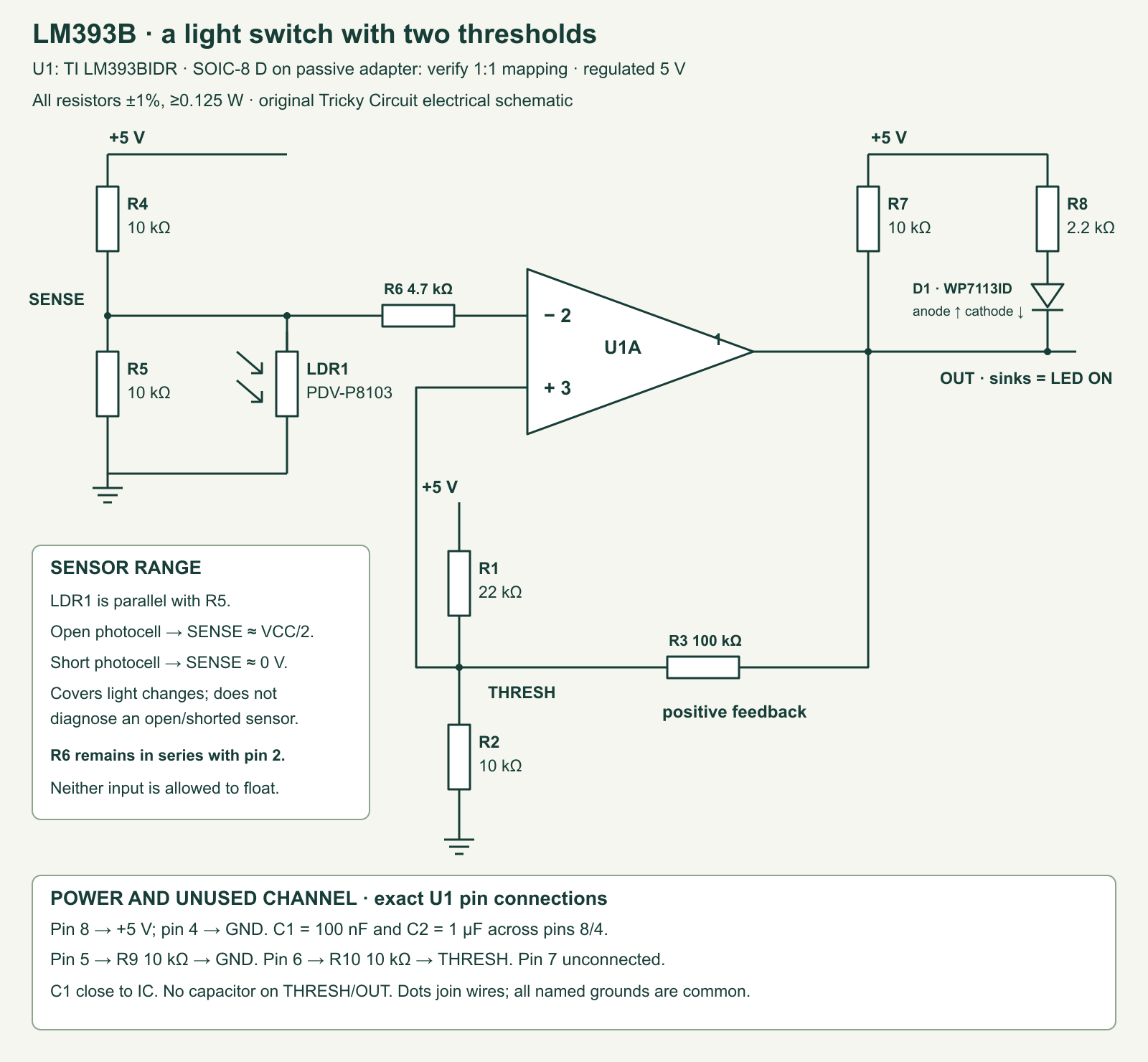
| Node | Exact connections |
|---|---|
| +5 V | U1 pin 8; R1 upper end; R4 upper end; R7 upper end; R8 upper end; C1/C2 supply ends. |
| GND | U1 pin 4; R2/R5 lower ends; LDR1 lower end; R9 lower end; C1/C2 ground ends; source negative. |
| THRESH | R1 lower end, R2 upper end, R3 feedback end, U1 pin 3, and R10 leading to pin 6. |
| SENSE | R4 lower end, R5 upper end, LDR1 upper end and R6 leading to U1 pin 2. |
| OUT | U1 pin 1, R3 output end, R7 lower end and D1 cathode. |
| LED branch | +5 V → R8 → D1 anode; D1 cathode → OUT. |
| Unused channel | Pin 5 → R9 → GND; pin 6 → R10 → THRESH; pin 7 left unconnected. |
Place C1 directly across pins 8 and 4 on the adapter, with a short return. C2 also spans the supply rails nearby. A bypass capacitor provides a short local route for rapid supply-current changes. Neither capacitor goes on THRESH or OUT. TI’s application guide explains that slowing the positive-feedback node can delay or defeat the intended hysteresis. Keep the output wire away from the sensitive input wiring; a breadboard’s accidental capacitance is not a designed feedback element.
LDR means light-dependent resistor. The PDV-P8103 has no electrical polarity. Its material is cadmium sulfide, abbreviated CdS; the exposed sensing face must receive the light. Treat the specified part as a light-sensitive resistor, not a calibrated lux meter. Lux is a measure of illumination weighted for human vision. Manufacturer resistance tests use a specified lamp spectrum and conditions; another lamp, orientation, temperature or photocell can give a different result.
R5 is essential: it stays in parallel with the photocell, so the sensor voltage cannot rise all the way to +5 V when the photocell becomes very resistive or is disconnected. R6 provides 4.7 kΩ in series with the minus input even if the photocell is shorted. The unused channel’s plus input reaches ground through R9, while its minus input reaches the positive THRESH voltage through R10. Its output transistor can remain sinking with its collector unconnected; no output pull-up is needed there. This follows the current TI guidance to give unused inputs a defined difference, avoid direct low-impedance input connections and leave unused outputs open.
Supply range and common-mode range are different
The LM393B can operate from a much wider supply than this project, but its inputs do not cover the entire positive supply range. Input common-mode range describes the allowed input-voltage region for specified comparator operation. The LM393B table gives ground to VCC−1.5 V at 25 °C and ground to VCC−2.0 V over −40 to +85 °C under the stated conditions. We keep both used input nodes inside the more conservative range. The datasheet also describes valid operation with one input outside that range when the other remains valid; this circuit does not need to rely on that allowance.
Our project supply window is 4.75–5.25 V. With nominal equal R4 and R5, the highest SENSE voltage is VCC/2: 2.5 V at 5.0 V. Including ±1% resistor extremes, the maximum ratio is 1.01/(0.99+1.01)=0.505. At the lowest supply, SENSE therefore stays at or below 2.39875 V, below the 2.75 V common-mode ceiling. THRESH stays around 1.4–1.9 V in the selected calculation cases. The unused pin 5 stays near ground and pin 6 near THRESH.
These margins are not permission to change the supply to 3.3 V while retaining the circuit: the full-temperature ceiling would then be only 1.3 V. Neither the 36 V recommended maximum supply nor the B version’s 38 V absolute maximum stress rating describes a valid input level for this 5 V experiment. A smaller board or similar LM393 marking does not establish identical limits, pin mapping or performance. No motor, relay, mains lamp or microcontroller input is attached here.
Calculate the two thresholds with the pull-up included
Call the THRESH voltage T and the OUT voltage O. Ignoring tiny input currents initially, the sum of resistor currents at THRESH gives:
(5 − T)/22000 + (O − T)/100000 = T/10000
T = (5/22000 + O/100000) / (1/22000 + 1/10000 + 1/100000)
In the sinking state, select O=0.200 V as an explicit example assumption. It is not a measured value or a promised low level at every input overdrive. The equation gives TLOW=1.47485 V. While brightening, SENSE must fall below this threshold to release the output and turn the indicator off.
In the released state, OUT is not exactly 5 V. R7 supplies current through R3 into the reference divider. With the LED nonconducting in this state, R7 and R3 act as a 110 kΩ path from +5 V to THRESH:
THIGH = (5/22000 + 5/110000) / (1/22000 + 1/10000 + 1/110000)
      = 1.76471 V
OUT_HIGH = 5 − 10000 × (5 − THIGH)/110000
         = 4.70588 V
Hysteresis width = THIGH − TLOW = 0.28985 V
Darkening raises SENSE. Crossing THIGH turns the output transistor on. OUT then drops and pulls THRESH down toward TLOW, reinforcing the sinking state. Brightening lowers SENSE and must cross TLOW to turn it off again. Between the thresholds, either output state can be stable: history matters. A circuit powered up inside that gap has no promised initial state. Begin each experiment from an input clearly outside the gap rather than inventing a startup memory.
The LED branch matters. When OUT is near 4.706 V, its available voltage is only about 0.294 V, so the simple red-LED model leaves that branch off. When OUT is assumed 0.200 V, a selected 1.9 V LED drop gives (5−0.2−1.9)/2200≈1.318 mA. R7 contributes 0.480 mA, and R3 contributes about 0.01275 mA. The total collector sink is approximately 1.811 mA. The 1.9 V value is an illustrative assumption: Kingbright specifies its listed forward voltage at 10 mA, while our current is much lower. Measure the actual LED and OUT voltages.
A useful current bound avoids assuming any LED drop at all. At 5.25 V and 1% low R8, R7 and R3, adding 5.25/2178, 5.25/9900 and 5.25/99000 gives less than 3.0 mA. That also pessimistically allows the full supply across the feedback resistor. The LM393B table specifies a low output of at most 0.4 V at 25 °C, or 0.55 V over its stated temperature range, at up to 4 mA sink and a −1 V differential-input test condition. Those test conditions matter: a barely crossed threshold is not automatically a −1 V overdrive. Use the current budget as a design screen and measure the settled output, especially near switching. R8’s worst zero-drop dissipation is below 13 mW, well below 125 mW.
Translate the threshold into resistance, not invented lux
The photocell lies in parallel with R5. With both fixed sensor resistors at 10 kΩ, the node calculation simplifies to:
SENSE = 5 × RLDR / (10000 + 2 × RLDR)
RLDR = 10000 × SENSE / (5 − 2 × SENSE)
Darkening trip:  SENSE = 1.76471 V → RLDR ≈ 12.00 kΩ
Brightening trip: SENSE = 1.47485 V → RLDR ≈ 7.19 kΩ
The manufacturer gives 16–33 kΩ at 10 lux under its specified 2856 K test light. That is already a broad range. We do not convert the two resistance thresholds into exact illumination thresholds or promise an identical night-light setting across parts. Position the photocell and establish the desired switching points by observation. The output LED must not shine on the photocell; an opaque divider between them prevents an unintended optical feedback path.
A disconnected photocell produces the same high-resistance direction as darkness and can light the indicator. A shorted photocell looks very bright. This circuit cannot distinguish those faults from real illumination. Hysteresis provides stable switching, not a supervised sensor-cable diagnosis. The photocell voltage never exceeds about half the supply in the intended circuit; the current-limiting network also keeps its calculated dissipation small. Do not remove resistors because the photocell’s absolute voltage rating looks large.
A repeatable memory experiment without changing the light
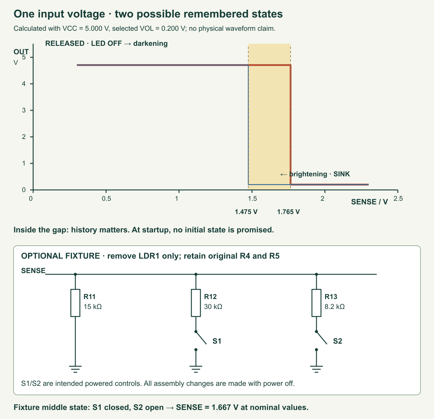
With power off, remove LDR1. Put R11=15 kΩ from SENSE to ground. Add R12=30 kΩ from SENSE through S1 to ground and R13=8.2 kΩ from SENSE through S2 to ground. These are three parallel branches replacing the photocell only; the original R5 remains. Use switches with their actual contact pairs checked by a continuity meter. Apply 5.00 V again after inspecting the connections.
- Leave S1 open and close S2. The replacement resistance is 15 kΩ in parallel with 8.2 kΩ, about 5.30 kΩ. SENSE is about 1.286 V, below TLOW; OUT should release and the LED should be off.
- Close S1, then open S2. The replacement resistance is now 15 kΩ in parallel with 30 kΩ: 10 kΩ. SENSE is 1.667 V, inside the window. OUT should stay released.
- Open S1. Only 15 kΩ remains in the fixture, giving SENSE=1.875 V. This crosses THIGH, so OUT should sink and the LED should light.
- Close S1 again. SENSE returns to the same 1.667 V used in step 2, but OUT should remain sinking. Measure both SENSE and OUT: the same input can now have a different output.
- Close S2. The additional branch lowers SENSE below TLOW and releases OUT again. Repeat the sequence and record actual voltages instead of replacing observations with the calculated examples.
The switches change only resistor-limited signal branches. Do not use this procedure as an excuse to move powered supply wires or short OUT to +5 V. Switch bounce can create brief intermediate transitions; pause after each step and examine the settled state. A meter can show the slow memory experiment, while an oscilloscope would be needed to investigate transition chatter. This static resistor model does not predict switch-bounce waveforms.
Measure the light thresholds and their limits
Power off, remove the entire fixture, and restore LDR1. Start with the photocell well illuminated; move a hand or an opaque card slowly to darken it. Record SENSE, THRESH and OUT just before and after the LED turns on. Continue darkening until the state is settled. Then brighten slowly and record the reverse transition. Keep the lamp type, direction, supply voltage and meter connections unchanged. Light level and photocell resistance can take time to settle, so repeat both sweeps rather than expecting two perfect numbers from one pass.
Use a meter with a high input resistance, ideally about 10 MΩ or greater, and record its range. Even that meter adds a small load to the node it touches. Do not insert its current terminals across the supply. Take resistance measurements only with power removed and the photocell disconnected from the parallel network; an in-circuit resistance reading includes R5 and other paths.
Resistor tolerances, output low voltage, comparator input offset, bias current and supply changes move the thresholds. Input offset voltage is a small equivalent input error; input bias current is the small current flowing at an input. The LM393B table lists a ±4 mV offset limit and 50 nA bias-current magnitude over its temperature range under the specified conditions. The two THRESH-connected inputs and the SENSE source resistance contribute additional small errors. The optional calculator explores ±1% reference/pull-up resistors, 4.75–5.25 V supply, selected 0–0.55 V OUT-low levels and an illustrative ±6 mV combined input-error allocation.
That enumeration is a selected-corner calculation, not a guarantee of a finished system over every condition. In particular, a fixed-drop LED approximation is not a semiconductor model, the photocell has its own temperature and history effects, and the low-output table uses a specified input overdrive. The calculator does not promise switching delay, noise immunity, brightness or measured accuracy. If added capacitance or long wiring changes the behaviour, inspect the actual waveforms and layout instead of using more decimal places.
Complete optional calculator and state model
Run with ordinary Python 3 on a host computer. No program is required for the physical analog circuit. The same functions below are exercised by the companion host tests; the state model preserves an UNKNOWN startup inside the gap. The optional --load parameter adds a hypothetical OUT-to-ground resistor to demonstrate how an unplanned output load changes the released level and threshold.
python3 code/lm393b_hysteresis.py
python3 code/lm393b_hysteresis.py --vol 0.35
python3 code/lm393b_hysteresis.py --load 10000
"""Original DC arithmetic for the article31 LM393B light switch.
No firmware, SPICE, propagation-delay or physical circuit simulation.
LED uses an explicitly assumed constant forward drop, not a device model.
"""
import argparse
import itertools
import json
import math
R_TOP = 22000.0
R_BOTTOM = 10000.0
R_FEEDBACK = 100000.0
R_PULLUP = 10000.0
R_LED = 2200.0
R_SENSOR_TOP = R_SENSOR_BOTTOM = 10000.0
def positive(value, name):
value = float(value)
if not math.isfinite(value) or value <= 0:
raise ValueError(name + " must be positive and finite")
return value
def nodes(released, vcc=5.0, vol=0.2, rtop=R_TOP,
rbottom=R_BOTTOM, rf=R_FEEDBACK, rp=R_PULLUP,
rled=R_LED, vf=1.9, load=None):
"""Solve threshold/output nodes, including pull-up and LED loading.
Released means the open-collector transistor is off. A hypothetical
load resistor connects OUT to GND; it is NOT fitted to the project.
"""
vcc = positive(vcc, "vcc")
if not 4.75 <= vcc <= 5.25:
raise ValueError("project supply range is 4.75 to 5.25 V")
vol, vf = float(vol), float(vf)
if not math.isfinite(vol) or not 0 <= vol <= 0.55:
raise ValueError("vol must be a selected 0..0.55 V assumption")
if not math.isfinite(vf) or not 0 < vf < vcc:
raise ValueError("vf must be positive and below vcc")
rtop, rbottom, rf, rp, rled = [positive(v, n) for v, n in
[(rtop, "rtop"), (rbottom, "rbottom"), (rf, "rf"),
(rp, "rp"), (rled, "rled")]]
gl = 0.0 if load is None else 1.0 / positive(load, "load")
gt, gb, gf, gp = 1 / rtop, 1 / rbottom, 1 / rf, 1 / rp
if not released:
out = vol
threshold = (vcc * gt + out * gf) / (gt + gb + gf)
led_current = max(vcc - out - vf, 0.0) / rled
else:
# Try the two constant-drop LED regions, and accept the one whose
# own solution satisfies its assumed conduction condition.
for led_on in (False, True):
gd = 1.0 / rled if led_on else 0.0
a, b, c = gt + gb + gf, -gf, vcc * gt
d, e, f = -gf, gp + gf + gl + gd, vcc * gp + gd * (vcc - vf)
determinant = a * e - b * d
threshold = (c * e - b * f) / determinant
out = (a * f - c * d) / determinant
if (vcc - out > vf) == led_on:
led_current = max(vcc - out - vf, 0.0) / rled
break
else:
raise ValueError("no consistent constant-drop LED solution")
pull_current = (vcc - out) / rp
feedback_current = (threshold - out) / rf
sink = pull_current + led_current + feedback_current - out * gl
if not released and sink < -1e-12:
raise ValueError("selected low voltage/load would require collector sourcing")
return {"threshold_V": threshold, "out_V": out,
"led_A": led_current, "pullup_A": pull_current,
"feedback_toward_out_A": feedback_current,
"collector_sink_A": 0.0 if released else sink}
def thresholds(**kwargs):
low = nodes(False, **kwargs)
high = nodes(True, **kwargs)
if low["threshold_V"] >= high["threshold_V"]:
raise ValueError("output loading destroys the intended hysteresis")
return {"brightening_release_V": low["threshold_V"],
"darkening_sink_V": high["threshold_V"],
"width_V": high["threshold_V"] - low["threshold_V"],
"released": high, "sinking": low}
def sensor_voltage(resistance, vcc=5.0, top=R_SENSOR_TOP,
bottom=R_SENSOR_BOTTOM):
top, bottom = positive(top, "top"), positive(bottom, "bottom")
vcc = positive(vcc, "vcc")
if resistance is None: # A disconnected photocell, not darkness proof.
return vcc * bottom / (top + bottom)
resistance = float(resistance)
if not math.isfinite(resistance) or resistance < 0:
raise ValueError("photocell resistance must be nonnegative and finite")
return vcc / (1.0 + top / bottom + (top / resistance if resistance else math.inf))
def resistance_at_voltage(voltage, vcc=5.0):
voltage = float(voltage)
if not math.isfinite(voltage) or not 0 < voltage < vcc / 2:
raise ValueError("voltage must be inside the nominal sensor range")
return R_SENSOR_TOP * voltage / (vcc - 2 * voltage)
class SwitchModel:
"""Ideal slow-state memory; UNKNOWN startup inside the hysteresis band."""
def __init__(self, state="UNKNOWN", **kwargs):
if state not in ("UNKNOWN", "RELEASED", "SINK"):
raise ValueError("invalid state")
self.state = state
self.vcc = kwargs.get("vcc", 5.0)
self.limits = thresholds(**kwargs)
def update(self, sense):
sense = float(sense)
if not math.isfinite(sense) or not 0 <= sense <= self.vcc - 2.0:
raise ValueError("sense outside selected full-temperature common-mode range")
if sense > self.limits["darkening_sink_V"]:
self.state = "SINK"
elif sense < self.limits["brightening_release_V"]:
self.state = "RELEASED"
return self.state
def corner_envelope():
"""Selected resistor/supply/VOL/error corners; not a system guarantee."""
lows, highs = [], []
for factors in itertools.product((0.99, 1.01), repeat=4):
for vcc, vol, error in itertools.product((4.75, 5.25), (0.0, 0.55), (-0.006, 0.006)):
t = thresholds(vcc=vcc, vol=vol, rtop=R_TOP*factors[0],
rbottom=R_BOTTOM*factors[1], rf=R_FEEDBACK*factors[2],
rp=R_PULLUP*factors[3])
lows.append(t["brightening_release_V"] + error)
highs.append(t["darkening_sink_V"] + error)
return {"cases": len(lows), "brightening_release_V": [min(lows), max(lows)],
"darkening_sink_V": [min(highs), max(highs)],
"note": "Selected independent corners; fixed-drop LED, no transient or lux model."}
def main():
p = argparse.ArgumentParser(description=__doc__)
p.add_argument("--vcc", type=float, default=5.0)
p.add_argument("--vol", type=float, default=0.2)
p.add_argument("--load", type=float, default=None,
help="hypothetical OUT-to-GND resistor, not fitted")
args = p.parse_args()
try:
result = thresholds(vcc=args.vcc, vol=args.vol, load=args.load)
result["nominal_photocell_trip_ohms"] = {
"brightening": resistance_at_voltage(result["brightening_release_V"], args.vcc),
"darkening": resistance_at_voltage(result["darkening_sink_V"], args.vcc)}
result["selected_corners"] = corner_envelope()
except ValueError as e:
p.error(str(e))
print(json.dumps(result, indent=2, allow_nan=False))
if __name__ == "__main__":
main()
The model solves the two connected nodes, including the pull-up path and the LED’s assumed conduction region. It does not silently set a released output to the supply. It rejects voltages outside this project’s supply window and rejects sensor inputs outside the selected full-temperature common-mode range. It is a DC arithmetic and memory experiment, not SPICE, firmware, or physical testing.
When the observations disagree
- Always lit: check for a disconnected photocell, poor sensor-ground connection, insufficient illumination or incorrect input pins. A dark indication alone cannot prove the sensor is connected.
- Never lit: check LED polarity and R8, measure OUT directly, and confirm THRESH changes when OUT changes. A reversed LED can hide a correctly switching comparator.
- One threshold instead of two: check R3 and its connection to the plus input. R3 to the minus input gives a different feedback arrangement. Check for an accidental capacitor on THRESH.
- Unexpected high level: inspect R7 and extra loads. The LED branch is not a substitute for the independent pull-up. A new board, indicator or probe can change the feedback calculation.
- Chatter: prevent the LED from illuminating the photocell, shorten input wires, verify the local supply capacitors and compare the actual input noise with the measured hysteresis gap.
- Unexpected current or warmth: switch off and recheck adapter pin mapping, shorts, resistor values and supply polarity. This experiment’s small resistor-limited loads should not heat the package noticeably.
Challenge: why is a released output not exactly 5 V?
Someone calculates THIGH by substituting O=5 V in the first equation and obtains a different threshold. Which current did they omit? Predict what happens if another 10 kΩ resistor is attached from OUT to ground.
Show the reasoning
They omitted the current through R7 and R3 into the reference divider. The released collector does not provide voltage; the external resistors determine it. R7 has about 29.4 µA flowing in the nominal released example, so it loses about 0.294 V. An extra OUT-to-ground resistor draws more current, reduces OUT and changes THIGH. It may also make the LED branch conduct in the released state. The supplied two-node calculator includes that hypothetical load, but the measured circuit must be checked again. Connecting arbitrary output loads is a design change, not a free indicator expansion.
Primary sources and related learning
Continue with the Tricky Circuit learning course and the loaded voltage-divider experiment. The same loading principle explains why the pull-up affects the released threshold.
- TI LM393 family datasheet, SLCS005AH, April 2025: exact pin functions, LM393B electrical table and operating versus stress ratings.
- TI LM393BIDR orderable-part page and product documentation: confirmed SOIC-8 package and current document list. No separately titled device errata was found in this review; recheck current documents before a substitution.
- TI application guidelines SNOAA35F, December 2024: input constraints, pull-ups, capacitors with hysteresis and unused-comparator termination, especially sections 6.11, 7, 8 and 9.1.
- Advanced Photonix PDV-P8103 and its Rev B manufacturer datasheet: named photocell and resistance test conditions.
- Kingbright WP7113ID V14A: LED identity, orientation and test conditions for its forward voltage.
Download the source package (ZIP): complete programs, full-size PNG and editable SVG diagrams, and the logger’s host tests. The same complete article program is included above.