An analog multiplexer lets several low-voltage signals share one analog input. Selecting the right address is only the first half of the job: the measurement node also has to move away from its previous voltage. Build an eight-way selector with a Pico, use three channels as a controlled experiment, and make the settling error large enough to investigate.
Verification status: the complete program and the calculations below were checked on a host computer, using mocks for the actual hardware interfaces. This design has not been assembled or executed on a Pico. The timing illustration contains an explicitly simplified model, not oscilloscope captures, and selected delays are experiment settings rather than guaranteed accuracy or switching specifications.
What the chip adds
A multiplexer, often shortened to mux, is a selector that joins one of several paths to a common terminal. The Texas Instruments CD74HC4051E contains eight bidirectional analog switch paths. “Analog” means that the selected path passes a continuously variable voltage; it does not turn the voltage into a digital reading. The Pico’s analog-to-digital converter (ADC) performs that conversion afterward.
Three digital address bits select a channel. A separate control input disconnects every channel when high. We call that input INHIBIT in this article; TI labels its pin E and describes active-low enabling. Keeping INHIBIT high while changing address prevents the program’s three individual pin writes from intentionally connecting intermediate channels. It is also the default state during startup and after the code exits.
One ADC reading still belongs to one selected instant. Eight channels do not become eight simultaneous samples, and the device does not isolate different grounds. The experiment uses one slowly adjusted potentiometer, one low reference and one high reference, all powered from the Pico’s own 3.3 V rail. It concentrates on address selection, source impedance, stored charge and honest reading status rather than becoming another calibrated multimeter.
Exact parts and orientation
Use TI CD74HC4051E, N-package PDIP-16, with the original, non-wireless Raspberry Pi Pico RP2040 and official RPI_PICO MicroPython v1.26.0. PDIP means plastic dual-inline package: two rows of through-hole pins. With the chip’s notch upward in a top view, pin 1 is at the upper left; numbering continues down the left edge and up the right. Check the marking and orientation before applying power.
The current TI datasheet reviewed for this lesson is SCHS122O, January 2026; its package addendum dated 7 October 2026 lists CD74HC4051E as PDIP N, 16 pins. The HC family’s recommended supply range includes 3.3 V. The HCT family has a different recommended range, so CD74HCT4051 is not the selected replacement. The manufacturer product page and datasheet were checked for a separate device errata notice; none was found in that review, which is not proof that no future or unpublished errata exists. TI product information, current datasheet.
The remaining parts are a 10 kΩ linear potentiometer, one 10 kΩ and one 100 kΩ interchangeable series resistor, two 1 kΩ reference resistors, a 5.6 kΩ upper and 1 kΩ lower divider resistor, three 100 kΩ address pull-downs, one 10 kΩ INHIBIT pull-up, a 100 nF supply bypass capacitor and a 10 nF C0G ceramic or film capacitor. Use ±1% resistors rated at least 0.125 W and capacitors rated at least 10 V; record the actual capacitor and pot tolerances. Add a breadboard, short jumpers and a Micro USB data cable. A potentiometer is a variable divider with two end terminals and a movable wiper.
Connections and component jobs
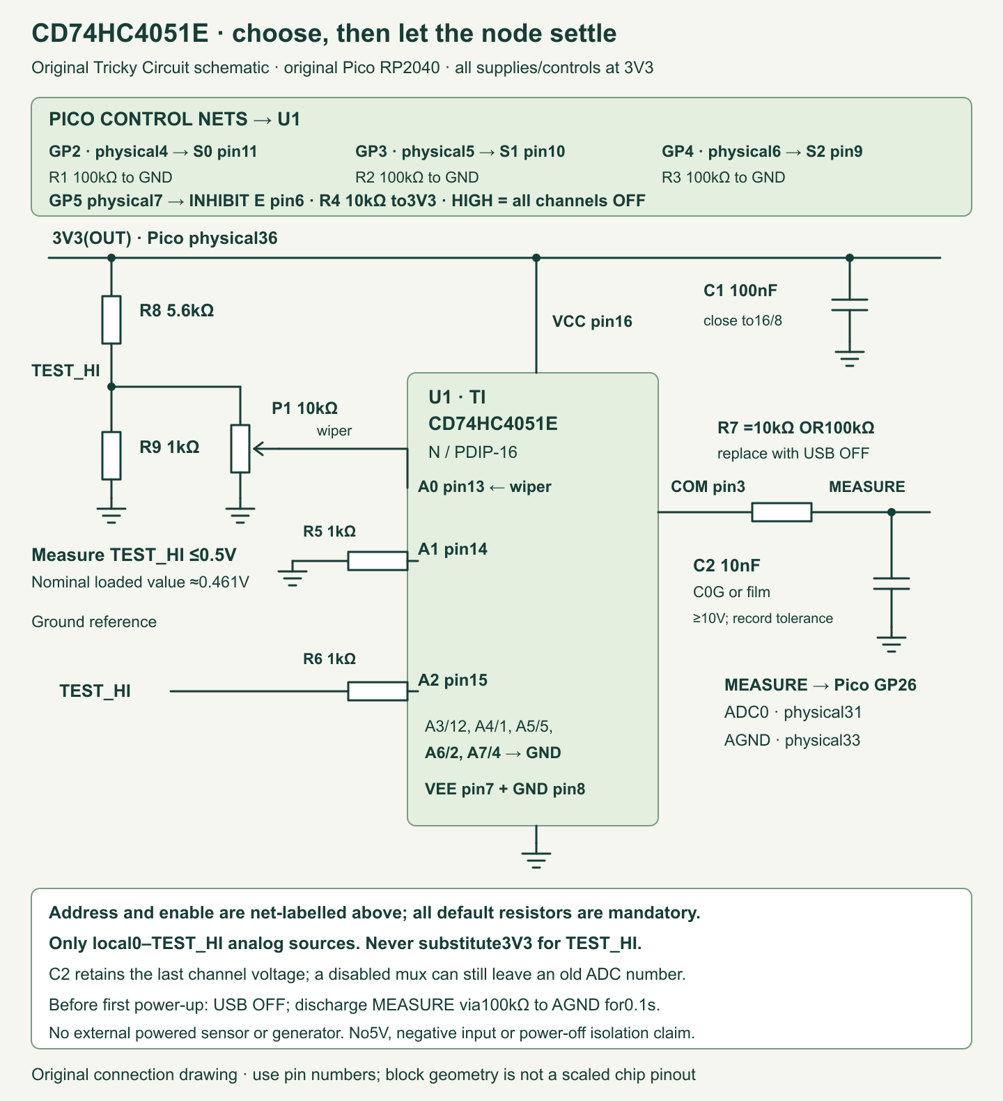
| TI pin | Function and exact connection |
|---|---|
| 16 VCC; 8 GND; 7 VEE | VCC to Pico 3V3(OUT), physical pin 36. GND and VEE both to ground; use Pico AGND physical pin 33 for the analog return. C1=100 nF directly between pins16 and8. TEST_HI is a separate divider output, not the supply rail. |
| 11 S0; 10 S1; 9 S2 | GP2 physical pin4; GP3 physical pin5; GP4 physical pin6. Each gets a separate 100 kΩ pull-down to ground. S0 is the least-significant address bit. |
| 6 E / INHIBIT | GP5 physical pin7; R4=10 kΩ pull-up to 3V3. High disconnects every analog channel. |
| 13 A0 | 10 kΩ potentiometer wiper; its two end terminals connect to TEST_HI and AGND. |
| 14 A1; 15 A2 | A1 through R5=1 kΩ to ground; A2 through R6=1 kΩ to TEST_HI. These provide contrasting source levels. |
| 12 A3; 1 A4; 5 A5; 2 A6; 4 A7 | Unused demonstration channels tied to ground, so none is left as a floating test input. |
| TEST_HI source | Pico 3V3 → R8=5.6 kΩ → TEST_HI → R9=1 kΩ → AGND. P1=10 kΩ track also connects between TEST_HI and AGND. Verify TEST_HI≤0.5 V before using the mux. |
| 3 COM | Through R7=10 kΩ initially, later 100 kΩ, to node MEASURE and Pico GP26/ADC0 physical pin31. C2=10 nF from MEASURE to AGND. |
GPIO means general-purpose input/output, the configurable digital pins carrying the address and inhibit signals. VCC is this chip’s positive supply, VEE its analog negative-supply terminal, and GND/AGND the ground reference. Grounding VEE makes this a single-supply experiment; it does not permit negative sensor voltages. Everything here stays between ground and the same 3.3 V rail. USB’s 5 V VBUS line is not an analog reference for this circuit.
The pull-up disables the mux before Python configures GP5. The pull-downs define address zero while the Pico address pins are inputs. C1 supplies short local current pulses and belongs close to the chip. C2 deliberately gives the ADC node memory of the previous channel. R7 makes that memory adjustable without changing firmware. The 1 kΩ reference resistors and R7 limit charging current; they are not precision voltage references. TI also cautions about voltage drop across a conducting switch in some current directions. Using the larger 10 kΩ baseline reduces that transient compared with a near-direct capacitor load; the actual switch voltage and current still need bench checking rather than an invented3.3 V Ron guarantee.
Check the transient condition as well as the rails. TI §5.4 footnote 3 cautions that switch drop must not exceed 0.6 V in some current directions to avoid extra VCC current. Our external capacitor sits after R7; its previous charge can oppose the newly selected source. Merely limiting current with R7 would not prove the switch drop from an assumed Ron. Instead, require TEST_HI≤0.5 V and use only this circuit’s 0–TEST_HI sources, with C2 initially discharged while power is off. Before first power-up or rewiring, temporarily connect MEASURE to AGND through the 100 kΩ spare resistor for at least 0.1 s, then remove that discharge connection. Never short the 3V3 supply directly. In the passive RC model every source and capacitor history stays within that span, so the instantaneous source-to-capacitor difference—and therefore any share across the switch—is below 0.6 V independently of Ron. Confirm the span and observe the node on a scope if available; do not apply external full-scale signals to this setup.
Use USB as the only power source. Do not connect an independently powered sensor, another board’s signal or a bench generator to an unpowered mux or Pico. INHIBIT does not make the analog pins tolerant of out-of-rail voltages or guarantee power-off isolation. Power down before rewiring, replacing R7 or removing the chip. Shared low-voltage rails and deliberate startup states are the basis of this tabletop design.
Calculate an experiment, not an accuracy promise
Source impedance describes how strongly a source resists a change in delivered current. Here the high source is a loaded divider, not an ideal rail. With ideal nominal resistors, its unloaded equivalent resistance is 5.6 kΩ∥1 kΩ≈848.5 Ω. At the 10 kΩ pot’s midpoint, the wiper sees 5 kΩ in parallel with (5 kΩ+848.5 Ω), about 2695.5 Ω. Across all pot positions the largest ideal equivalent is about 2712.1 Ω. Component tolerances and wiring change this; a generic “pot resistance divided by four” would overlook the divider source.
The selected switch contributes on-resistance, Ron, which varies with supply, signal level, temperature and device. Do not copy the front-page 70 Ω typical figure into a guaranteed 3.3 V calculation: that figure belongs to a 4.5 V test condition. The detailed tables also do not provide a 3.3 V guaranteed Ron row. This lesson uses 1000 Ω only as a declared model assumption for exploring sensitivity; it is neither a measured value nor a promised upper bound for this chip.
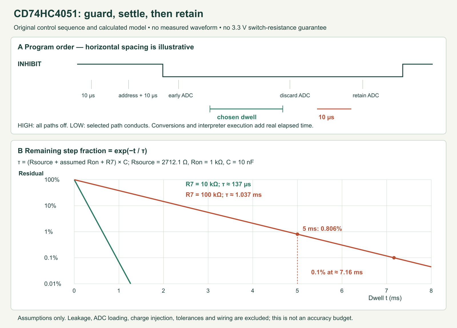
A simple resistor–capacitor, or RC, model gives τ = (Rsource + Ron + R7) × C2. The Greek letter τ, tau, is the time constant. Using the largest nominal source equivalent above, the assumed Ron and nominal 10 nF, R7=10 kΩ gives τ≈137 μs; R7=100 kΩ gives τ≈1.037 ms. After a voltage step, the model’s remaining fraction is exp(−t/τ). Five milliseconds in the slower example leaves approximately 0.806% of the initial step: about 3.7 mV of a 0.461 V test step. This is why “I waited a little” needs a numerical definition.
In that simplified slow case, reducing the remaining fraction below 0.1% would require ln(1000)≈6.91 time constants, or about 7.16 ms. This does not establish system accuracy. Ron was assumed, the capacitor and source have tolerances, leakage can create a persistent error, and the Pico’s ADC and reference have their own limitations. Waiting removes transient error; it does not calibrate a steady offset.
The RP2040 ADC samples through a small switched capacitance, approximately 1 pF in its datasheet, with additional board and package capacitance. C2 is deliberately much larger and can act as a local charge reservoir, but it also stores the previous channel’s voltage. A diagnostic early conversion and later discarded conversion can themselves disturb that node. They are observations of this setup, not a universal “discard one sample and accuracy is fixed” rule. MicroPython’s read_u16() returns a scaled 0–65535 result; that API range does not turn the RP2040’s native 12-bit converter into a 16-bit-accurate instrument. RP2040 ADC description, MicroPython ADC API.
Complete program and reading status
Install the pinned official firmware for the original Pico, keep a local copy of this program, then save it on the board as main.py. MicroPython is the Python interpreter running on the Pico. The interactive USB prompt is a REPL, or read–evaluate–print loop. Confirm the firmware banner before running the experiment. Host validation does not install or execute firmware on the board.
Each sample disables the mux, waits 10 μs, writes S0 then S1 then S2, waits another 10 μs, enables the selected path and takes one explicitly diagnostic early conversion. After the chosen dwell it discards one conversion, waits 10 μs and retains the next. The finally block requests disabled state after success, failure or interruption while the board still executes and Pin operations function. It cannot guarantee an output state after power loss or damaged hardware; the external pull-up provides the default when GP5 is high impedance. These guard values are conservative experiment settings; they are not newly invented3.3 V guaranteed switching specifications.
"""TI CD74HC4051E + original RP2040 Pico; MicroPython v1.26.0.

All power and analog sources come from the Pico's same 3V3/GND rails.
Settle delay is an experiment setting, not a guaranteed error specification.
"""

DISABLE_US = 10
ADDRESS_US = 10
ADC_GAP_US = 10
DWELL_US = 5000
STALE_MS = 1000


def checked_raw(value):
    if type(value) is not int or not 0 <= value <= 65535:
        raise ValueError("ADC result outside read_u16 range")
    return value


class MuxReader:
    def __init__(self, address, inhibit, adc, clock):
        if len(address) != 3:
            raise ValueError("S0,S1,S2 pins required in least-significant order")
        self.address = address
        self.inhibit = inhibit
        self.adc = adc
        self.clock = clock
        self.records = [None] * 8
        self.inhibit.value(1)

    def sample(self, channel, dwell_us=DWELL_US):
        if type(channel) is not int or not 0 <= channel <= 7:
            raise ValueError("channel must be 0..7")
        if type(dwell_us) is not int or not 0 <= dwell_us <= 50000:
            raise ValueError("dwell_us must be 0..50000")
        record = dict(channel=channel, early=None, raw=None,
                      acquired_ms=None, attempted_ms=self.clock.ticks_ms(),
                      dwell_us=dwell_us, status="READ_ERROR")
        try:
            self.inhibit.value(1)
            self.clock.sleep_us(DISABLE_US)
            for bit, pin in enumerate(self.address):
                pin.value((channel >> bit) & 1)
            self.clock.sleep_us(ADDRESS_US)
            self.inhibit.value(0)
            # Diagnostic conversion can itself disturb the sampling node.
            record["early"] = checked_raw(self.adc.read_u16())
            self.clock.sleep_us(dwell_us)
            checked_raw(self.adc.read_u16())  # discard one conversion
            self.clock.sleep_us(ADC_GAP_US)
            record["raw"] = checked_raw(self.adc.read_u16())
            record["acquired_ms"] = self.clock.ticks_ms()
            record["status"] = "ACQUIRED"
        except OSError:
            # Never retain the previous number as a fresh result after failure.
            record["early"] = None
            record["raw"] = None
        except ValueError:
            record["early"] = None
            record["raw"] = None
            record["status"] = "VALUE_ERROR"
        finally:
            self.inhibit.value(1)
        self.records[channel] = record
        return dict(record)

    def snapshot(self, channel):
        if type(channel) is not int or not 0 <= channel <= 7:
            raise ValueError("channel must be 0..7")
        record = self.records[channel]
        if record is None:
            return dict(channel=channel, status="NOT_READ", raw=None, early=None)
        result = dict(record)
        if result["status"] == "ACQUIRED":
            age = self.clock.ticks_diff(self.clock.ticks_ms(),
                                        result["acquired_ms"])
            result["age_ms"] = age
            if age < 0 or age >= STALE_MS:
                result["status"] = "STALE"
                result["raw"] = None
                result["early"] = None
        return result


def run(machine_module=None, clock=None, dwell_us=DWELL_US, emit=print):
    if type(dwell_us) is not int or not 0 <= dwell_us <= 50000:
        raise ValueError("dwell_us must be 0..50000")
    if machine_module is None:
        import machine as machine_module
    if clock is None:
        import time as clock
    m = machine_module
    # External 10k pull-up holds inhibit high before this line executes.
    inhibit = m.Pin(5, m.Pin.OUT, value=1)
    address = ()
    try:
        address = tuple(m.Pin(n, m.Pin.OUT, value=0) for n in (2, 3, 4))
        adc = m.ADC(m.Pin(26, m.Pin.IN, pull=None))
        reader = MuxReader(address, inhibit, adc, clock)
        while True:
            for channel in (1, 2, 0):  # low reference, high reference, knob
                result = reader.sample(channel, dwell_us)
                # sample() has already disabled the mux before USB output.
                emit("ch=%d state=%s early=%s raw=%s dwell_us=%d t_ms=%s" %
                     (channel, result["status"], result["early"], result["raw"],
                      dwell_us, result["acquired_ms"]))
            clock.sleep_ms(250)
    finally:
        inhibit.value(1)
        # External resistors retain disabled/default state when pins float.
        for pin in address:
            pin.init(mode=m.Pin.IN, pull=None)
        inhibit.init(mode=m.Pin.IN, pull=None)


if __name__ == "__main__":
    run()
ACQUIRED means that the program received an in-range conversion after its configured procedure. It does not mean the selected dwell has been proven sufficiently accurate. Each record carries its channel, dwell and completion timestamp. snapshot() changes an older record to STALE after 1000 ms and hides its old raw value. READ_ERROR and VALUE_ERROR also expose no reading. Age uses wrap-aware ticks_diff comparisons: call snapshot regularly, within half the platform’s tick-counter period; it cannot reconstruct an age after an arbitrarily long unattended gap. A zero conversion is valid numeric data; a failed read is not silently converted to zero.
The program’s channel order 1→2→0 alternates the low reference, high reference and knob. This intentionally creates large transitions. Changing the order can change early readings because the measurement capacitor retains history. Only three records are printed per scan; there is no growing list, file write or unbounded retry loop. USB output occurs with the mux disabled. It may lengthen the actual scan period, which is why the code does not advertise a fixed sampling frequency.
Bench procedure
- Inspect with power removed. Confirm chip orientation, VEE and GND both grounded, separate default-state resistors, bypass placement and all five unused inputs grounded. Fit R7=10 kΩ. Never select a part merely because a bag says 4051.
- Confirm reference behavior. Before enabling the mux, measure TEST_HI with a meter and confirm it is at most 0.5 V. Start with a 20000 μs dwell. The low reference should be near the ADC’s bottom end; the high reference should represent about 0.461 V nominal, only roughly 570 native 12-bit counts above ground. Do not expect a full-scale count or demand exact endpoint numbers. Turn the pot slowly and check that channel0 follows it. If channel identities or control states are wrong, repair those before interpreting settling.
- Make the node slower. Disconnect USB, replace only R7 with 100 kΩ, reconnect and leave C2=10 nF fitted. Keep TEST_HI≤0.5 V; never substitute 3V3 for this divider output. Place the pot near the opposite end from the preceding high reference to emphasise the step. No separate powered signal source is needed.
- Sweep one variable. Repeat runs with
DWELL_USset to 0,100,1000,5000 and 20000. Record early and retained counts, pot position, R7, capacitor value/tolerance, reference order and actual observations. Because Python and conversion overhead remain, the zero-dwell test is not literally a zero-time physical sample. - Look for a plateau. Compare the retained values across longer dwells, reverse channel order as a separately labelled trial, and return R7 to10 kΩ after powering down. A change with dwell or previous channel supports a settling/history explanation; a persistent shift at all dwells needs a different investigation.
If you have a high-input-impedance oscilloscope probe, inspect MEASURE relative toAGND and record how the probe changes the circuit. Its capacitance adds to C2. Without an oscilloscope, the printed observations still form a useful experiment, but they do not reveal the full transient or prove that no fast disturbance occurred. Keep measured results separate from the article’s model.
Leakage, crosstalk and practical limits
Leakage is unwanted small current through a nominally off path or an input. A high source resistance turns even a small leakage current into an offset: ΔV = Ileak × R. As a sensitivity example, 100 nA through 100 kΩ produces 10 mV. That 100 nA is a chosen example, not the complete device’s guaranteed worst-case3.3 V leakage. Long dwell cannot remove a voltage error that is maintained by continuous current.
Crosstalk means a changing unselected signal influences the selected one, through parasitic capacitance or shared wiring. Charge injection is a small charge disturbance associated with switching. The TI analog-performance figures have their own test conditions; they do not certify this breadboard, capacitor and ADC combination at an arbitrary frequency. Low-impedance sources, short analog routing, good grounds and suitable buffering can matter more than adding arbitrary averages.
The supply range and analog input range are operating constraints, distinct from absolute-maximum stress ratings. A catalog headline such as “±5 V analog range” assumes an appropriate supply arrangement and cannot be applied to this 0–3.3 V build. Likewise a mux neither amplifies a weak source nor limits an external overvoltage to a safe ADC value. An independently powered sensor needs a separate, verified interface design.
The four-point MiniMeter lesson uses a different ADC arrangement and discusses sequential time skew. The site’s learning course supplies supporting circuit basics.
What the local checks establish
The validator imports the exact supplied code. Its mocked mux rejects address changes while enabled, checks all eight binary addresses and ensures every conversion is associated with the selected path. Tests inject read errors, invalid ADC values and interruptions, exercise the actual running loop, verify inhibit cleanup and startup order, and check stale records across a wrapping clock. The RC calculations use a separate explicit mathematical model. None of these tests measures real Ron, validates a firmware binary or claims physical settling time.
Challenge: Why can a longer dwell leave the same wrong result?
If the error is the capacitor’s incomplete transient, more time should reduce it under otherwise unchanged conditions. If it comes from leakage through a large source resistance, a wrong reference, the ADC’s offset, a miswired channel or an out-of-range source, the final equilibrium itself may be wrong. Compare several dwell values, channel orders and a lower source resistance before attributing every mismatch to speed. The mux selects a path; it does not decide whether the source’s voltage means what you think it means.
Primary references
- TI SCHS122O, January 2026: CD74HC4051E PDIP pinout, HC/HCT operating distinctions, truth table, Ron conditions, analog restrictions and bypass guidance. Package addendum 7 October 2026.
- TI CD74HC4051 product page: exact product and documentation review.
- Original Raspberry Pi Pico datasheet: physical pin assignments and supply connections.
- RP2040 datasheet, ADC section 4.9: native converter and sample input behavior.
- MicroPython ADC v1.26.0 and Pin API: exact program interfaces.
Download the experiment sources (ZIP): complete programs, full-size PNG and editable SVG diagrams, and blank worksheets where supplied. The complete article program remains inline above.